Introduction
Vector network analyzer (VNA) are used to measure scattering parameters of high frequency circuits. When frequency is high enough the reflections of the waves start to matter and distributed effects need to be taken into account. VNA can be used to analyze reflection and transmission coefficients of circuits at high frequencies.
For example ideally antenna would radiate all the energy it gets, but all antennas reflect some of the energy back to the source and only radiate energy at certain frequencies. With VNA amount of energy reflected as function of frequency can be measured. Amplifiers also reflect some energy from both input and output and have some amount of gain. All of which can be measured using VNA.
Unfortunately VNAs are often very expensive and way out of my budget. Newest cutting edge VNAs with very wide frequency band can have insanely high cost. For example starting price of Anritsu's 110 GHz VectorStart ME7838A VNA is $575,850. Even used VNAs for lower frequencies are often several thousand dollars. At ebay cheapest used 6 GHz two port VNAs seem to sell for about 2,000€, still way more than I'm willing to pay.
Since I can't afford even a used VNA I decided to make one myself with a budget of 200€, tenth of what they cost used and about 1/100 of what they cost new. Of course it isn't going to be as accurate as commercial VNAs, but I don't need that high accuracy and it's a good learning experience anyway.
Block diagram
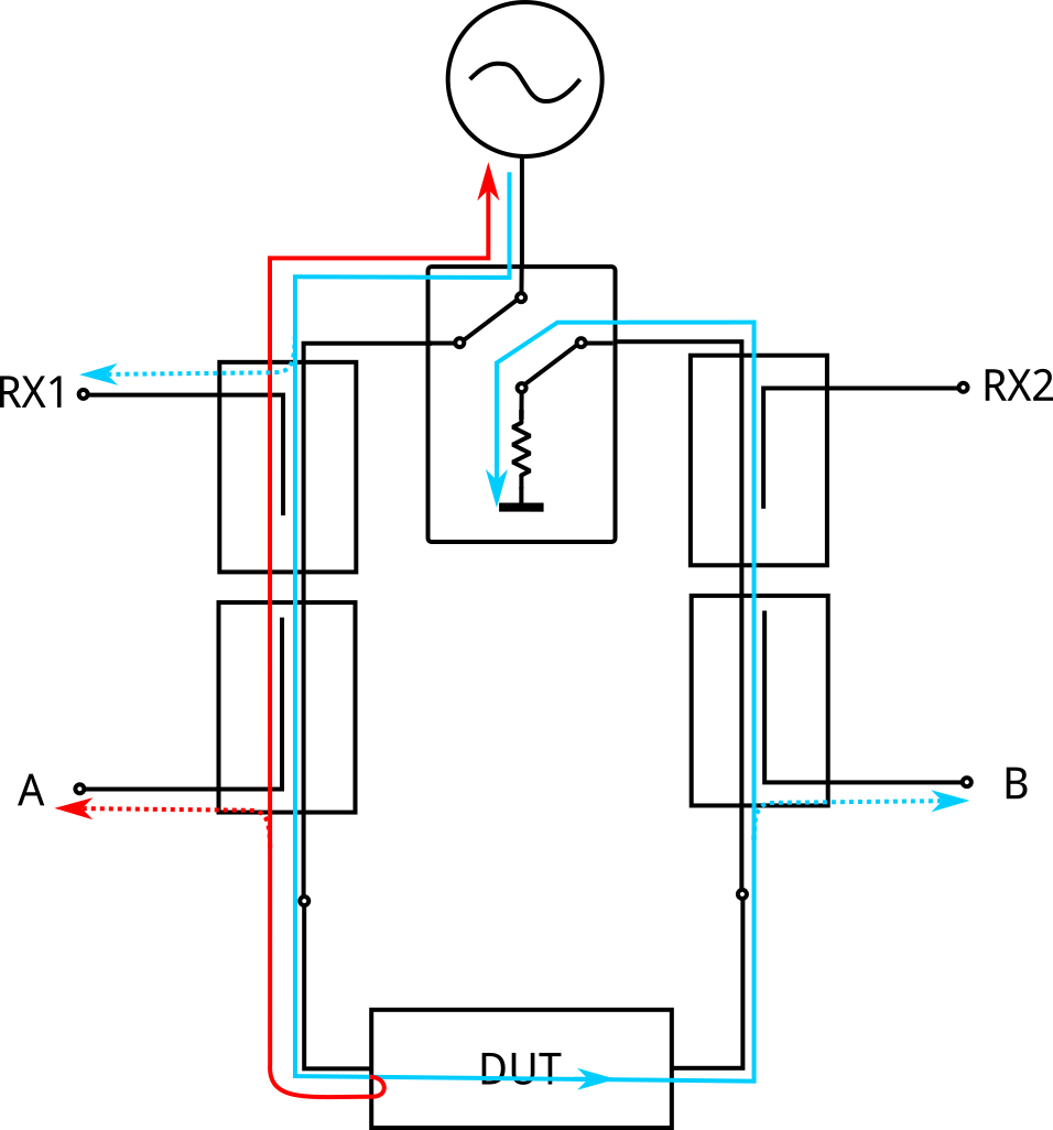
General block diagram of VNA.
So how does VNA measure reflection and transmission of signals? Operating principle is simple, but implementation is more challenging. Theoretically VNA consists of signal source that is used to excite the device under test (DUT), two directional coupler per port that measure transmitted and reflected waves and detectors at the end of the couplers that can measure both amplitude and phase of the signals.
Signal source generates a test signal which is routed to one of the ports. Part of the signal is coupled by the receiver directional coupler and its phase and amplitude are measured. Rest of the signal goes out of the VNA port and into the device under test. Some of the signal is reflected back to the source port and it is measured by another directional coupler. Ratio of reflected power to transmitted power is used to calculate the reflection coefficient of the DUT.
Non-reflected part of the signal goes through the DUT and can either be attenuated or amplified after passing through the device. When the test signal comes out of the DUT, part of the signal is coupled by the directional coupler on the second port and its phase and amplitude are measured. Rest of the signal passes to the termination where it is absorbed. Transmission coefficient is calculated as ratio of received power to transmitter power.
When measurement is repeated with the source switch connected the other way, reflection and transmission coefficients of the DUT can be measured from the other direction.
However in practice measurement isn't so simple. Biggest difference is length of the transmission lines inside the VNA and cables connecting the DUT causing loss and affection the measured phase. At 6 GHz wavelength on PCB is about 3 cm. For the phase difference between receivers to negligible distances from source, couplers and DUT should be much smaller than that. Especially cables connecting the VNA to the DUT need to be much longer than that so that device can be connected. There is also losses on cables, couplers and transmission lines inside the VNA. Directional couplers aren't perfectly directional and they couple also some signal coming from the other direction. Source and load matching aren't going to be perfect and will also reflect some signal back. There are also reflections from the internal components of the VNA. All of the errors also have some frequency dependence.
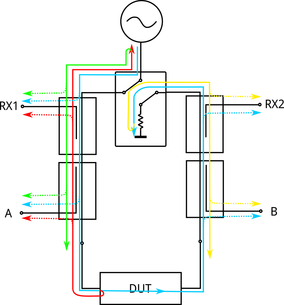
Block diagram with some of the error sources drawn.
However situation isn't hopeless as all of the error terms can be solved from measurements of devices with known reflection and transmission coefficients. When error terms are known, real reflection and transmission coefficients can be solved from the measurements. Usually very accurately characterized short, open and load standards are measured on both ports and through line is used to calibrate the transmission from port to port.
Four receiver VNA
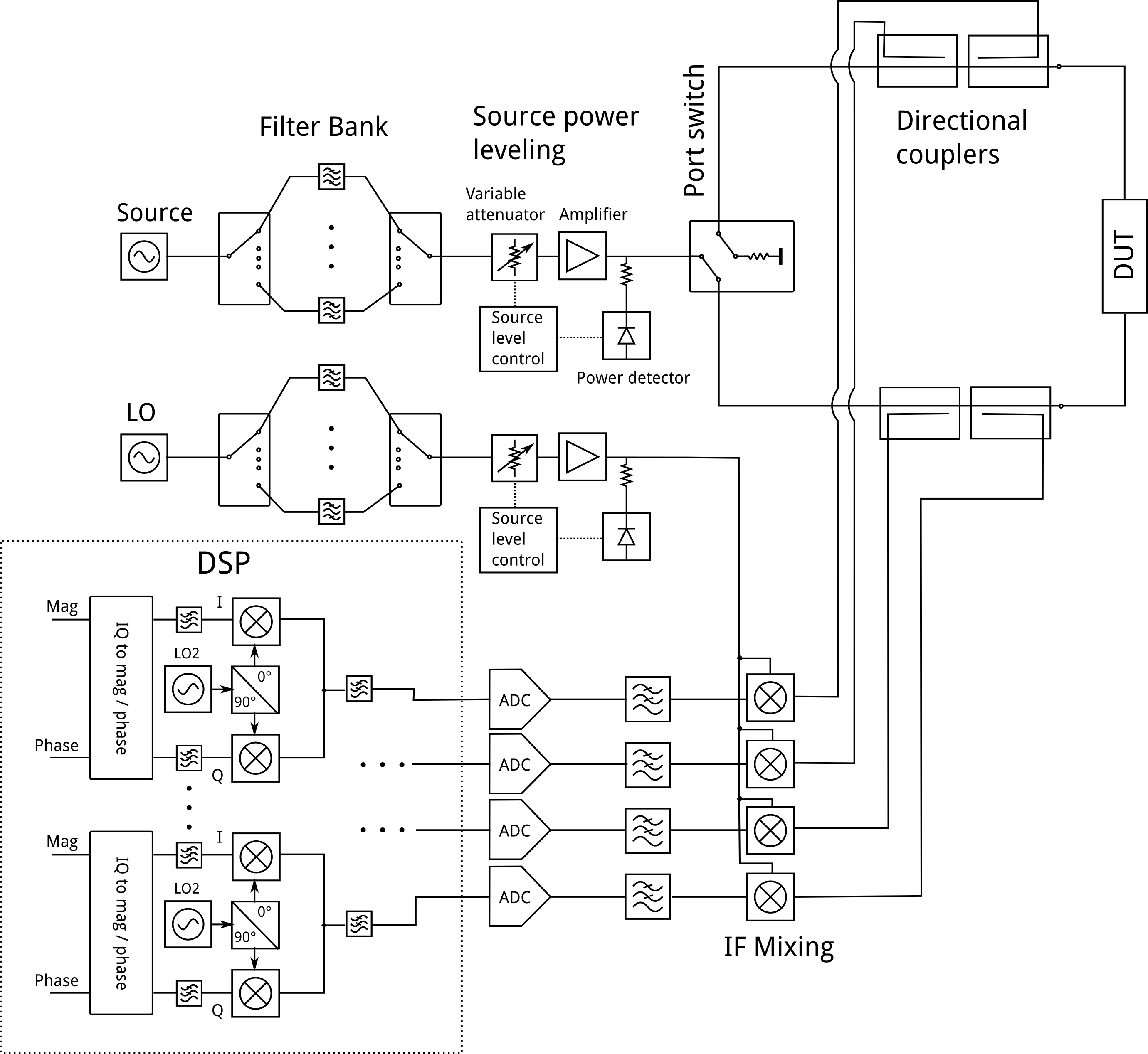
Block diagram of common two port, four receiver VNA. Most of the commercial VNAs work like this.
If you want to see a more detailed block diagram of VNA, take a look at for example PNA-X Service Manual N5242-90001. On page 119 there is a very detailed block diagram of the RF parts. Above is a simplified version of the diagram.
Source is implemented using a phase locked loop and often frequency multipliers are used to reach the higher frequencies. To keep the output power level constant as a function of frequency, output power after the output amplifier is measured and attenuator before the amplifier is adjusted until the sensed power is correct.
Power coupled into the directional couplers is high frequency and it needs to be mixed down before it can be detected. Super heterodyne receiver with one intermediate frequency is often used receiver architecture that avoids complications with mixing straight to the DC. In this case the signal exists only at one frequency and this allows setting the intermediate frequency very low, about few MHz, and doing the final mixing digitally. Digital mixing has advantage over analog implementation in that while no analog component can be perfect, digital mixing can be made as accurately as needed. Analog mixers add noise, phases of the LO signals of two mixers aren't perfectly equal, performance varies as a function of temperature and operating voltage and so on. None of these errors exist with digital mixing and measured result is much more accurate.
While this is a good architecture for making a VNA, it has a drawback of needing many expensive components. 30 MHz - 6 GHz mixer costs about 10€, high accuracy ADCs about 10 - 20 €, fast microcontroller, or better, FPGA is needed to interface to the ADCs, control switches, toggle other signals and communicate with computer. Just these components cost at least 100 € and many more components are still needed such as PLLs, oscillators, filters, PCBs, power converters and so on. Whole board would be way too expensive so something has to be removed to save money.
Single receiver VNA
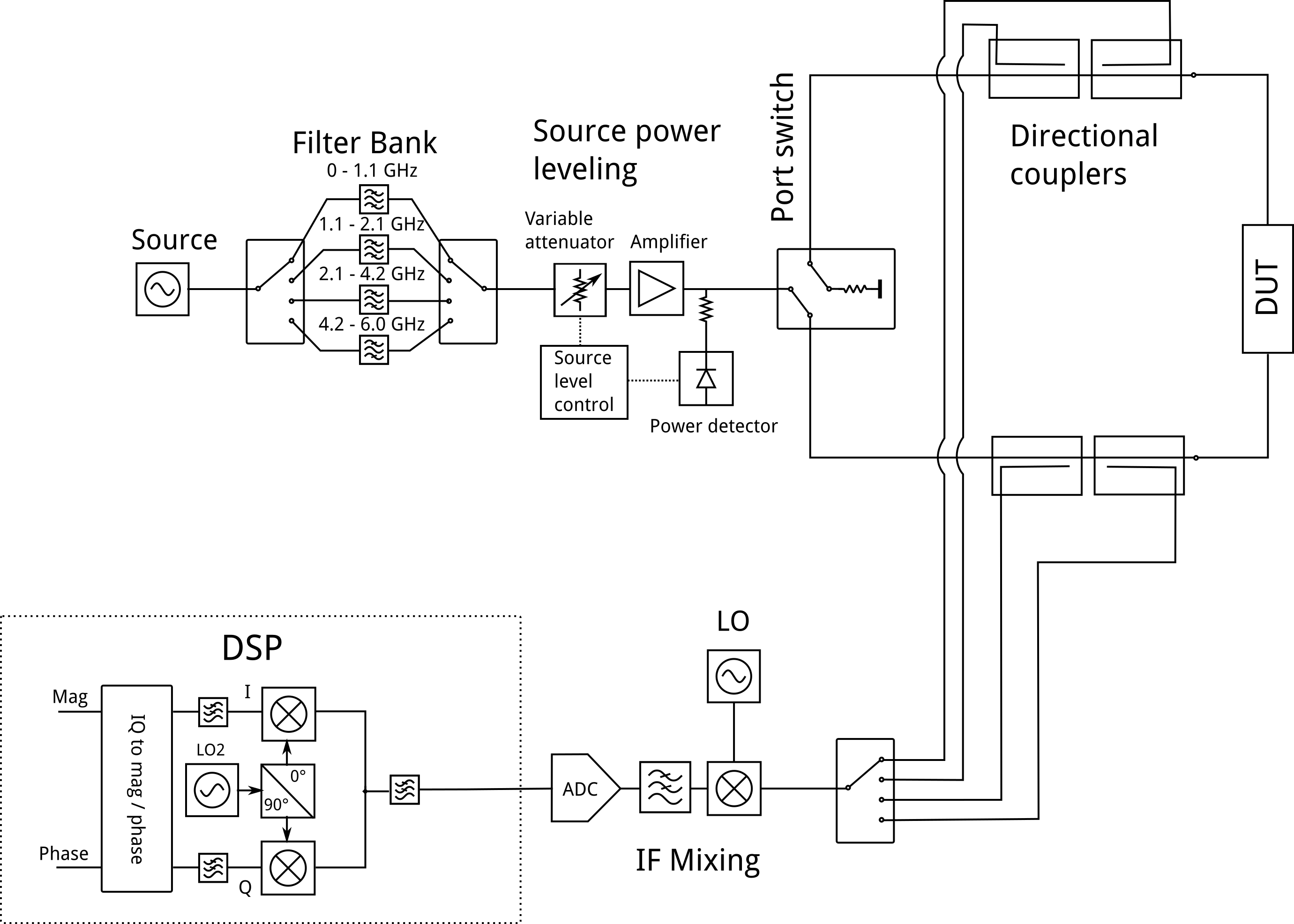
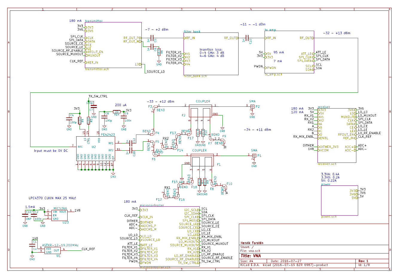
Block diagram of my VNA.
Most radical way to simplify the block diagram is replacing the receivers with single receiver and SP4T switch. This removes three ADCs, mixers and filters while adding a single switch. Signal processing is also simplified since now we must only measure one ADC instead of four. This change does have some drawbacks. Firstly the SP4T switch isn't perfect and it will have some leakage between the receiver channels. In theory it can be calibrated out, but it will reduce dynamic range of the measurements. Secondly previously all of the four channels could be measured at the same time, but now only one channel can be measured at once. This increases the time required to measure a single frequency sweep by four times.
Local oscillator can also be simplified as harmonics and exact power level doesn't matter that much as long as it is withing the specifications of the mixer.
In practice leakage from the SP4T switch is going to be a problem with calibration. Normal VNAs use high quality components and crosstalk between the ports can be assumed to be non-existent. With this architecture unless care is taken to minimize the crosstalk (which would require increased cost), it can't be assumed to be zero. Normal calibration procedures are unable to correct for it and there will be errors in the final measurements. There are more complicated special calibration procedures that can correct the leakage, so calibrating is still possible.
Design
Directional coupler
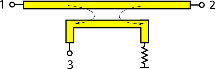
Coupled line coupler. When wave is passed from port 1, most of it goes through to the port 2 and some of it will be coupled to the port 3. When wave is passed from port 2, most of it will again go through to port 1, but some of it will couple. This time the coupled wave will be absorbed by the termination resistor and ideally nothing is detected on port 3.
The heart of the VNA are the directional couplers. In theory they can be made simply with two lines side by side with small gap between them. When a high frequency wave passes through one of the lines some signal couples to the nearby line. The coupled wave also prefers to go in one direction and ideally nothing would go to the other direction, but in reality there is small signal also to the other direction. Ratio of how much power goes to right direction compared to the power going to the wrong direction is called directivity. A good coupler can have directivity of more than 30 dB (one thousandth of power going to the wrong direction).
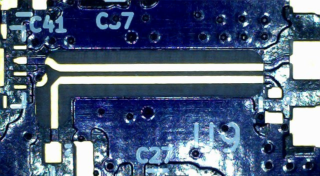
Microstrip coupler from my radar.
How does the directivity affect the accuracy of VNA? If the directivity is 0 dB, then the coupler can't really be called directional anymore and transmitted and reflected waves can't be separated. Result is that VNA can't measure anything. If the directivity is poor, but above 0 dB, there is some error in the measurements. It can be calibrated out, but the dynamic range of receiver is limited and accuracy is reduced. So for accurate VNA we need to have as high directivity as possible.
Turns out that stripline coupler, where lines are on the internal layers of the PCB, can be made with higher directivity than microstrip coupler where lines are on the top side of the PCB. I don't really know the exact reason myself, it has something to do with that on microstrip one side is PCB with high relative permittivity and other side is air with lower permittivity. Stripline on the other hand is embedded inside PCB and so it has same material on both sides.
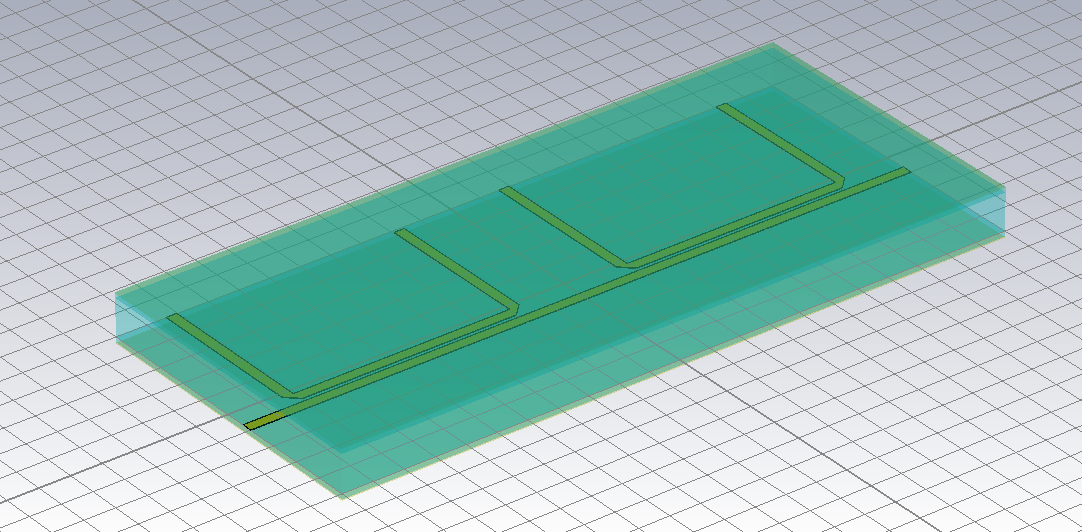
3D simulation model of two stripline directional couplers.
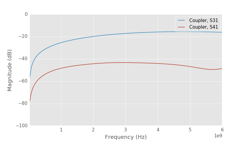
Simulated coupling in forward (S31) and reverse (S41) directions. S-parameters are plotted with scikit-rf python package.
Simulated directivity is 20 dB at low frequencies and 30 dB at high frequencies. Coupling decreases very rapidly at lower frequencies due to coupling lines being electrically very short compared to wavelength. Coupling at low frequencies can be improved by making a multi-stage coupler. I decided to not make one, because it would have required more PCB area and even single stage couplers are pretty big. As a result of it dynamic range at low frequencies is going to be poor. I'm more interested at high frequencies so reduced accuracy at lower frequecies doesn't matter too much.
There is still a potential problem with making a connection from microstrip trace on the top side to internal layer of the PCB. A via is needed, but does it work with low enough reflections at these frequencies?
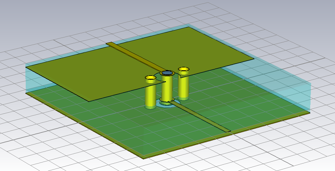
3D simulation model of via.
I made a simulation of a via structure with one signal via and two ground vias close to it. It's important to add ground vias close to the signal via so that ground current can also change layers without needing to go too far.
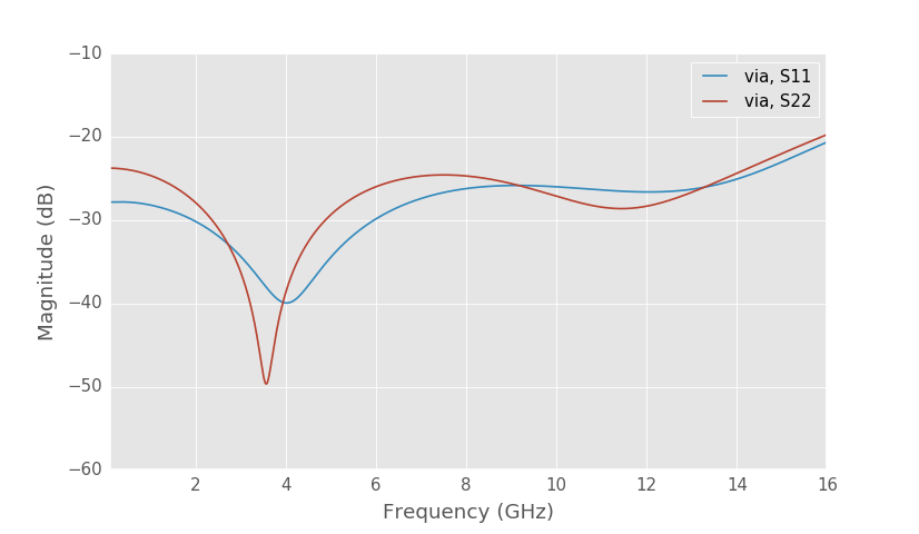
Simulated return loss of the vias. Insertion loss is about 0.4 dB.
According to the simulations there doesn't seem to be any problems with this kind of via connection and return loss is very good. I even simulated it up to 16 GHz and according to the simulation it still works well at that frequency.
Source and local oscillator

PLL block diagram.
To accurately generate frequencies at GHz range a phase locked loop is needed. It can generate accurate signals using a feedback loop that compares output frequency of voltage controlled oscillator (VCO) divided by N to stable low frequency reference clock. Feedback loop tries to make these frequencies equal by adjusting the tuning voltage of the VCO. Result is that output frequency of the VCO is N times the reference clock frequency. By cleverly changing the divider value fractional division values can be realized.
Problem with wideband signal generation using PLL is that good quality voltage controlled oscillators are usually not very wideband. To generate signals over wide bandwidth there are several different options:
- Frequency multipliers and dividers can be used to extend frequency range. Disadvantage of this approach is that they both generate high number of harmonics so filtering is needed.
- Two PLL outputs can be mixed together to generate sum and difference frequencies. This also generates harmonics and needs a second PLL and mixer.
- Multiple switched VCOs can be used. This requires logic for choosing a correct VCO and of course many VCOs are needed.
Luckily this problem has already been solved and there are several commercial PLL chips with integrated VCO bank and output frequency dividers. Some suitable ones are ADF4355 which can generate output frequencies from 54 MHz to 6.8 GHz and MAX2871 which can generate frequencies from 23.5 MHz to 6.0 GHz.
MAX2871 is a cheaper choice and it has a suitable frequency range, so I choose to use that. It has multiple VCOs and frequency dividers. Especially at lower frequencies frequency dividers can generate high harmonics and some filtering is needed to clean the signal. Because frequency band is so wide multiple filters are needed to cover it all without passing harmonics. I decided to use four filters working at 0 - 1.1 GHz, 1.1 - 2.1 GHz, 2.1 - 4.2 GHz and 4.2 - 6.0 GHz. More would be better especially at lower frequencies, but they would soon become too expensive compared to the advantage of having them. Four is a good choice from cost perspective, since RF switches with more than four poles are often more expensive than switches with less poles as there are less use for such switches. Connecting multiple switches in series is possible, but would need more PCB area.
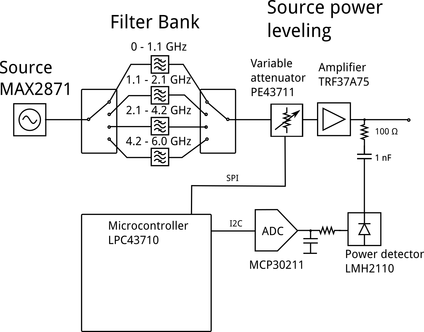
More detailed block diagram of the source.
After the filters there is power leveling circuits consisting of variable attenuator, RF amplifier and power detector.
Variable attenuator is PE43711 that can be configured to have attenuation from 0 dB to 31.75 dB in steps of 0.25 dB.
RF amplifier needs to be very wideband, I chose to use TRF37A75 RF amplifier. It's a cheap 40 to 6000 MHz amplifier with 12 dB gain. Gain is very stable as function of frequency, it varies only about 3 dB over the whole frequency range. Output matching however could be better as it is only -7 dB at 6.0 GHz and reflections from the amplifier output will cause some errors in measurements. Now that I think it would have been a good idea to add some places for matching components so that matching could be improved afterwards, but it's too late for that now.
At the amplifier output there is a power detector connected using a 100 ohm resistor. The resistor works as a -10 dB coupler and capacitor is used for DC blocking.
Microcontroller is used as a part of the feedback loop. It could be done using operational amplifier based circuit, but it can't be used in this case. Power level of the source must remain constant during the measurement of different receiver channels or else there will be uncorrectable errors in the measurements.
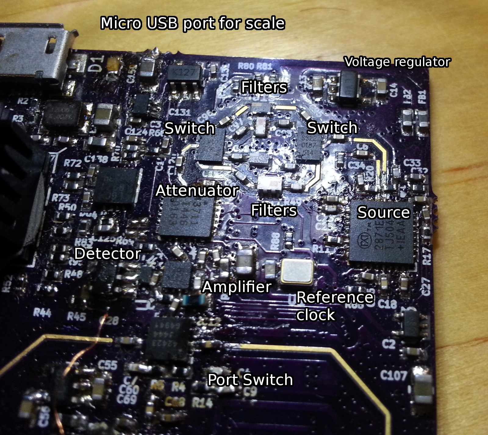
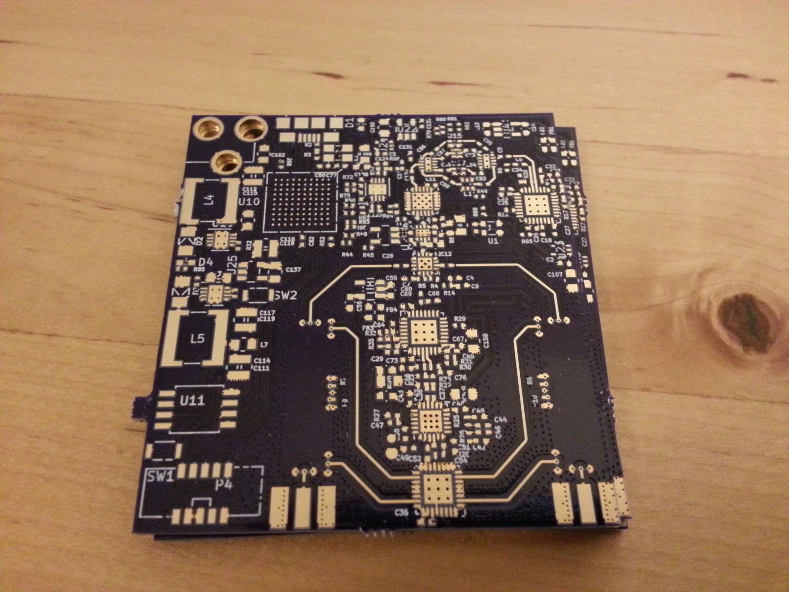
PLL, filters and power leveling circuits on PCB. PLL has its own voltage regulator to reduce interferences. Big component under the detector text is actually ADC. Detector is the small 1.2 x 0.8 mm black box right of it.
Above is a picture of the source components on PCB. Especially around the amplifier area the components couldn't be placed more closely together. I even placed some DC blocking capacitors at 45 degree angle so that I could save few mm of space. I decided to add power leveling only after routing the rest of the PCB so space got little tight.
Local oscillator uses another MAX2871 chip to generate signal for the receiver mixer. Filtering this signal isn't necessary as harmonics don't degrade performance of the mixer. Power leveling isn't needed either as long as the power level stays within correct range. For accurate frequency generation it's important to use same reference clock for both source and LO. ADC sampling clock should also be derived from the same reference for the best accuracy. If they were to use different references, they could drift relative to each other. Using same reference means that even if the reference drifts, it will cancel out after sampling as all the frequencies drift the same amount.
Receiver
Receiver consists of SP4T switch, mixer, local oscillator, anti-aliasing filter and ADC.
Switch causes crosstalk between the channels reducing the accuracy of measurements. A very high isolation switch would be ideal for the best performance. Low loss is also welcome as high loss reduces the dynamic range, but high isolation is more important. Switch also needs to be absorptive instead of reflective on non-switched ports and of course work from 30 MHz to 6 GHz.
It would also be possible to use three SP2T switches and it would probably give better isolation. However single SP4T switch is simpler and optimizing performance isn't that critical. It's better to keep design simple at this point and optimize performance in next revisions.
I chose to use Peregrine PE42441 SP4T switch that has about 40 dB isolation. It does affect the accuracy, but hopefully not too much. Commercial VNAs have often very high >100 dB isolation between the ports, so this is very poor compared to them.
To my knowledge there is only one possible affordable mixer that can be used over the whole frequency range. It is the same ADL5801 mixer that I used on my radar.
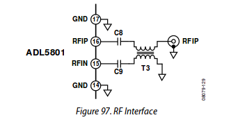
Recommended mixer input connection.
Mixer has a balanced input and datasheet recommends using a balun to convert single-ended signal to differential signal for mixer input. Issue is that most of the baluns are narrowband, while this application needs a balun capable of operating over the whole frequency range from 30 MHz to 6 GHz. There is one balun from MiniCircuits that is capable of operating over the whole frequency range, but it costs 7€ a piece and I would need to order it directly from MiniCircuits.
Other option is to leave the balun out and drive the mixer single endedly. Other unused output is connected to ground through a capacitor. Since single ended input impedance of mixer is 25 ohms and the system impedance is 50 ohms, return loss of the mixer is going to worsen. Conversion gain and linearity will also suffer. It does however save 7€ (+shipping) and PCB area so it seems worth it.
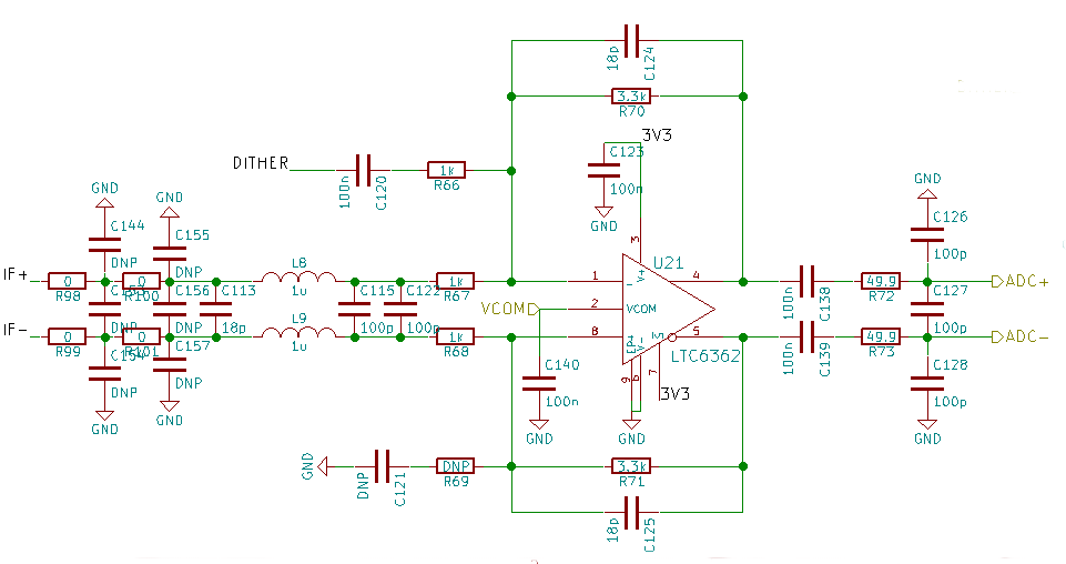
IF filter.
LO frequency is set to 2 MHz below (or above, doesn't matter) source frequency. This gives a 2 MHz IF signal which is easy to sample and filter. On my radar filter could have been more aggressive and this time I added some optional filtering components that can be added if needed. Differential amplifier buffers the signal for ADC and slightly amplifies it. Final RC filter before ADC further attenuates high frequencies above sampling frequency to avoid aliasing.
DITHER signal is a noise signal that can be added to ADC input. Why add deliberately noise to the signal? Consider the case where signal to be measured is so small that peak-to-peak value is less than one ADC least significant bit. Then the ADC might only output constant value and nothing is detected. If a noise signal is added then some changes are always seen at the ADC output. This time the signal to be measured can affect the output value of ADC. If noise and signal have different frequencies then the noise signal can be filtered out. Since signal affected some of the output values it can be detected after filtering. So by adding noise dynamic range of the ADC was increased.
Find out more at this Analog devices article.
Good idea, but turns out that due to leakage between the channels there is always enough signal to be detected so it isn't needed.
Digital logic
Microcontroller (or FPGA) is needed on board to handle communication with computer and control all the devices. Since only one ADC is needed with the switched receivers I decided to save money and look for a microcontroller with integrated ADC.
Most suitable one I could find was NXP LPC4370. It has one ARM-Cortex M4 core and two Cortex-M0 cores, high speed (480 Mb/s) USB support and 80 MHz 12-bit ADC. Maximum clock frequency is 204 MHz, so it should be fast enough.
This part has the fastest integrated ADC that I have seen on any microcontroller. External ADCs with same clock rate and bit depth cost more than this whole microcontroller, so the cost savings are considerable. It's available in hobbyist unfriendly 100 and 256 ball BGA packages.
Voltage regulation
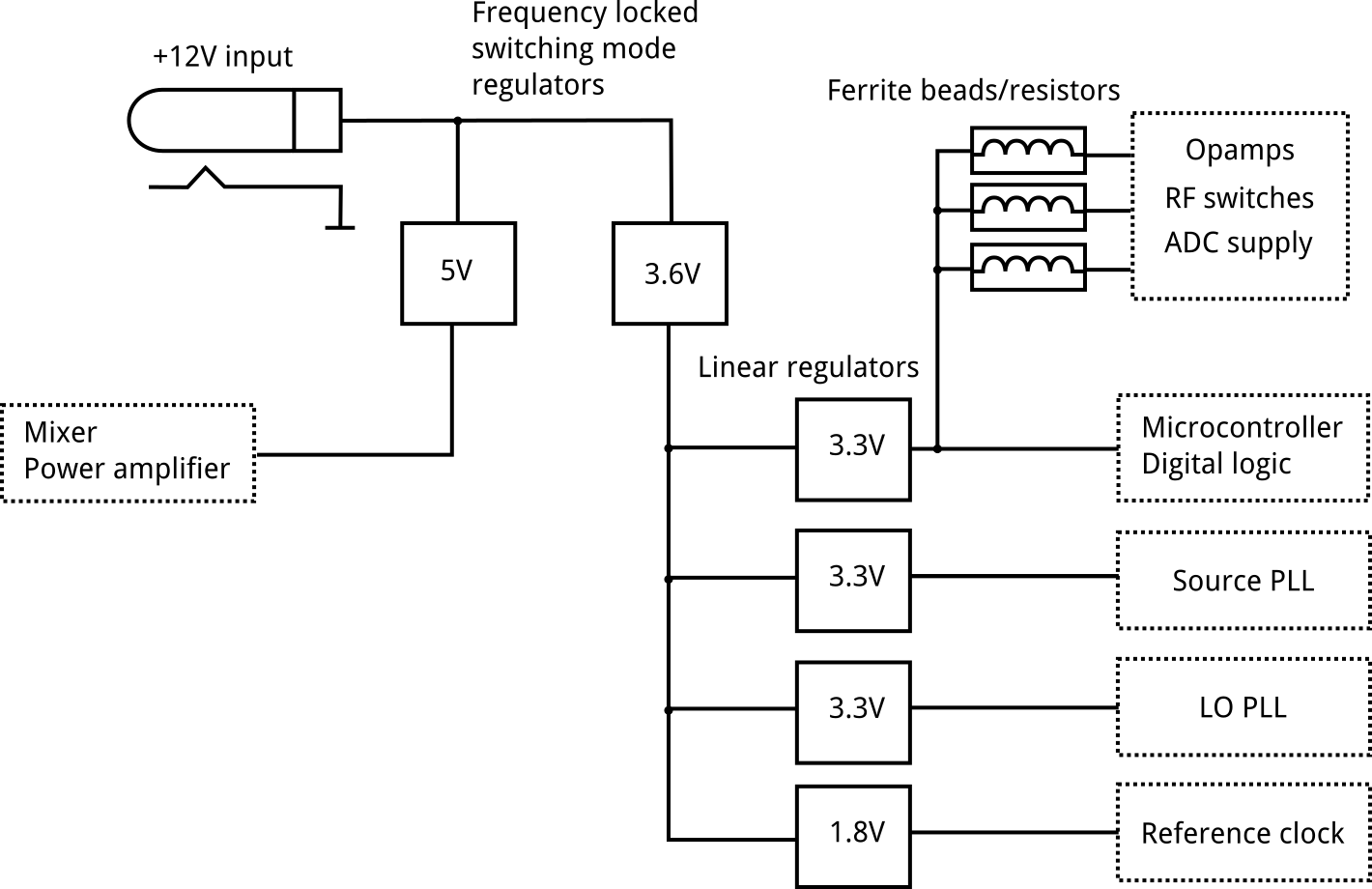
Block diagram of power supplies.
For high accuracy measurements it's important that there is no noise on the power supply that can make its way into the signal path. For my radar I made a mistake of using switching mode power supply for analog parts and ADC. While the noise was not very high, it was still detectable.
This time I decided to pay extra attention into the power supply design to minimize interferences. Still I didn't want to go too far, since high quality components can be expensive. For example shielding the RF parts would be helpful, but would cost too much.
Switching mode power supplies.
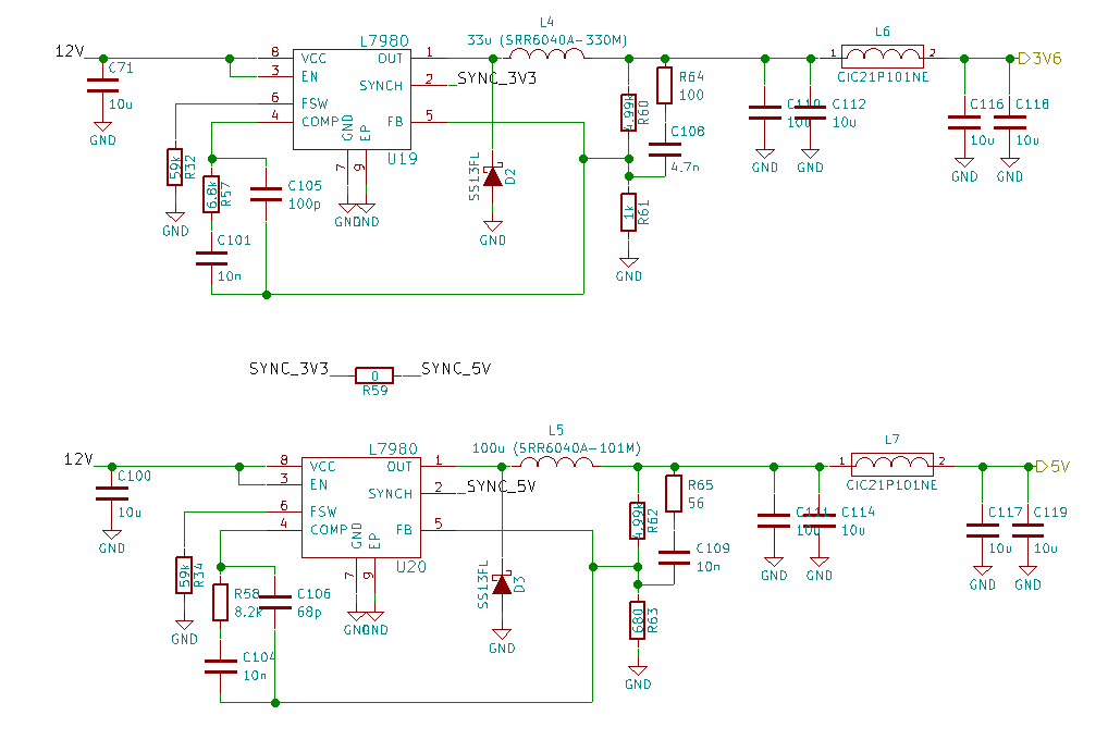
Power consumption of the board is about 3 W. Power consumption limit from USB bus is 0.5 W, so external supply is needed. 12 V is common AC adapter output voltage so I chose to use that as input voltage. There is some filtering right after the DC plug after which power goes to two L7980 switching mode power converters. Special feature of L7980 regulator is that switching frequencies of two different regulators can be synchronized by connecting two pins on the regulators together. Switching frequencies will synchronize in such a way that phase difference between the regulators is 180°. This results in lower input ripple as current draw from the input filtering capacitors is spaced apart. Having synchronized switching frequency is useful as there is noise only at one frequency on both 5V and 3.3 V rails.
If the frequencies wouldn't be synchronized mixing products of the different switching frequencies could be created. One path which this can happen is that if the power inductors are placed close to each other magnetic fields on the inductors can couple and switching noise is injected between them causing sum and difference terms of the switching frequencies to be detected at outputs of both of the regulators. Another path that switching noise can travel is through the shared input. As regulator switches it draws current and input voltage decreases a little bit. Because regulators share input voltage, noise is injected to output of the other regulator.
Care must also be taken when connecting a linear regulator after a switching regulator. Goal of this connection is usually to have good efficiency of the switching regulator and low noise of the linear regulator. Noise reduction can be much less than thought if power supply rejection rate (PSRR) of linear regulator isn't high enough at the switching frequency.
For example if we place MCP1700 3.3 V linear regulator after switching power supply that has a switching frequency of 100 kHz we will find that adding the linear regulator had barely any effect. Switching noise after the regulator is same as before it.
If we replace the linear regulator with LP5907 the switching noise after the linear regulator is gone. What's the difference between these two linear regulators?
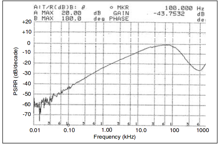
PSRR of MCP1700.
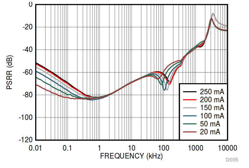
PSRR of LP5907.
Looking at the power supply rejection rate plots on the datasheets of the devices we find that at 100 kHz MCP1700 has PSRR of about 0 dB. All the noise at this frequency just passes through. LP5907 has PSRR of -60 dB. For example a very large 0.1 V noise at the input would only be 100 µV at the regulator output.
MCP1700 does still have use cases. It is much cheaper and would be a good choice for powering digital systems where noise doesn't matter that much.
Schematic and layout
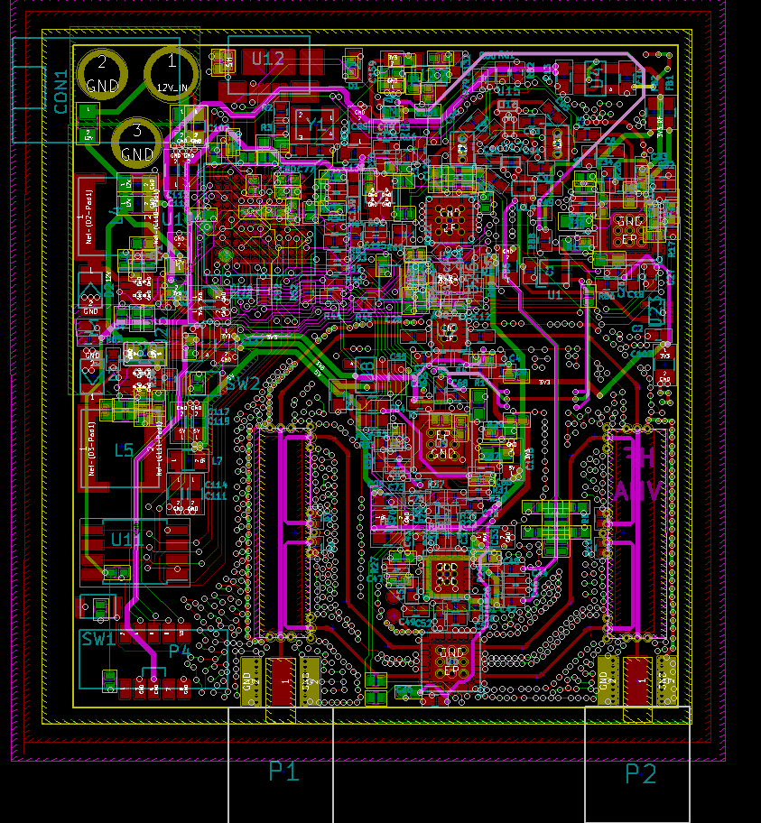
Layout in KiCad.
PCB was designed with KiCad. New push-and-shove router is really helpful when routing a tight board like this.
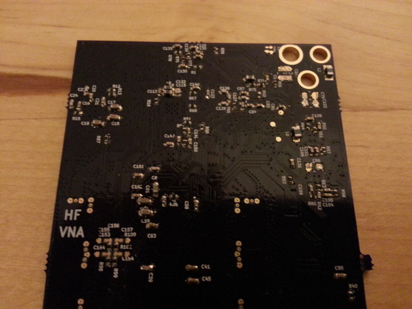
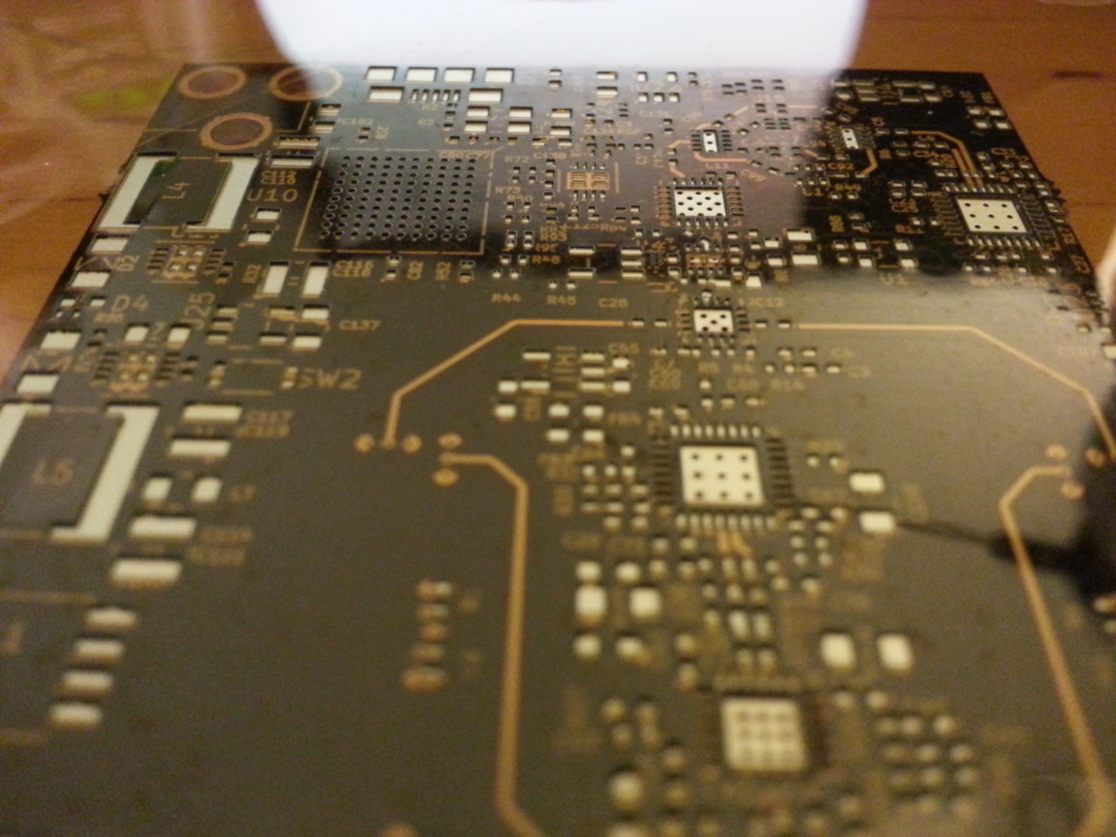
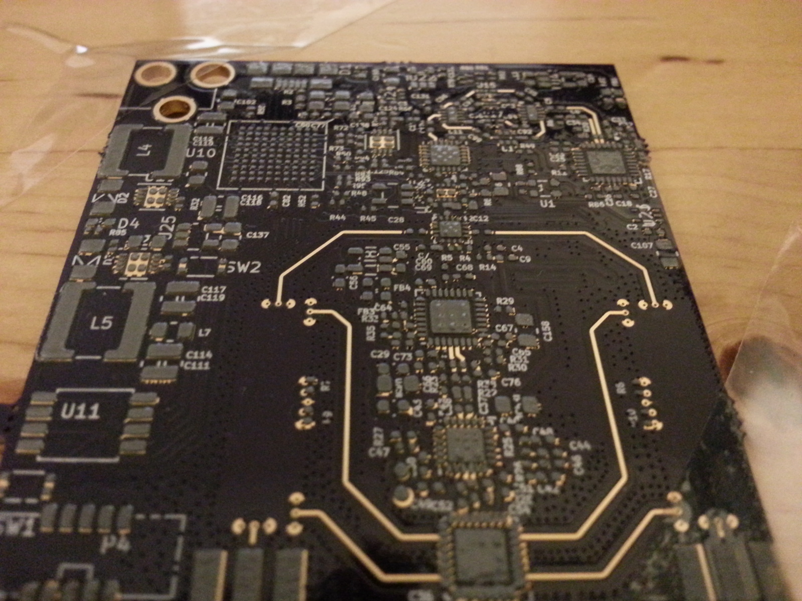
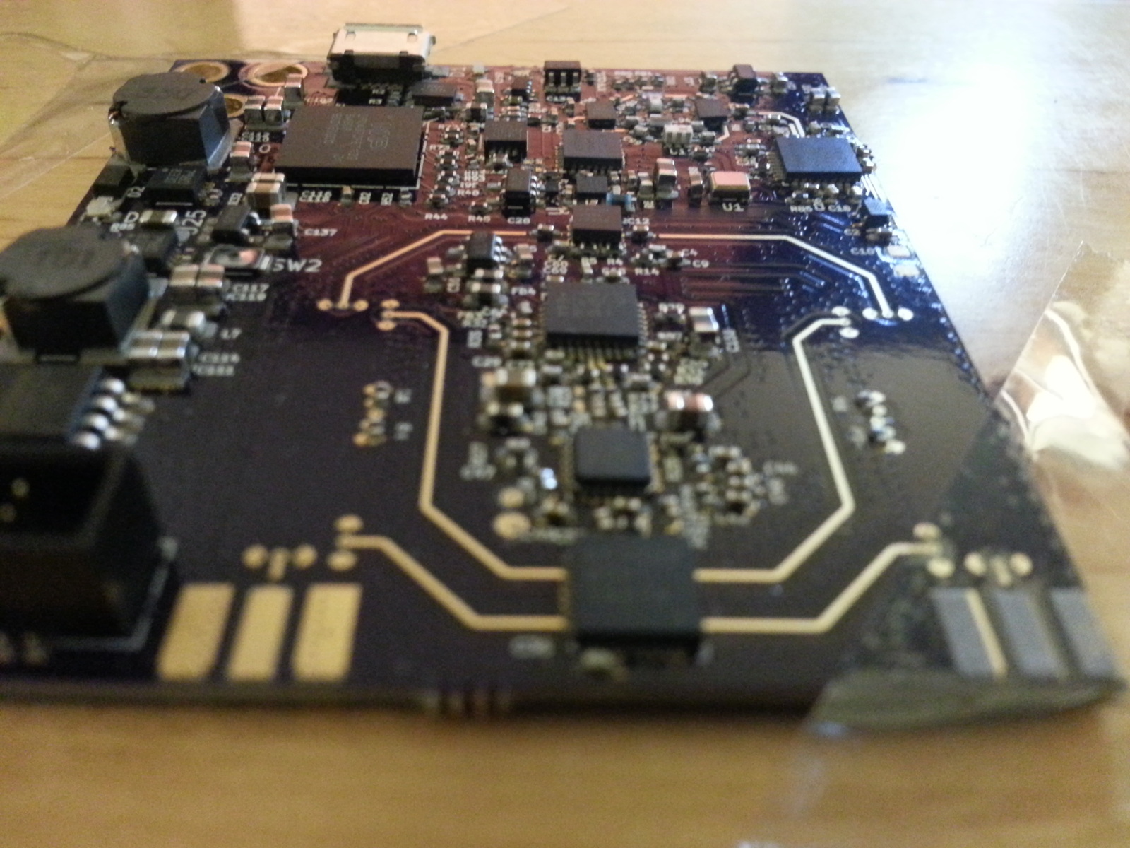
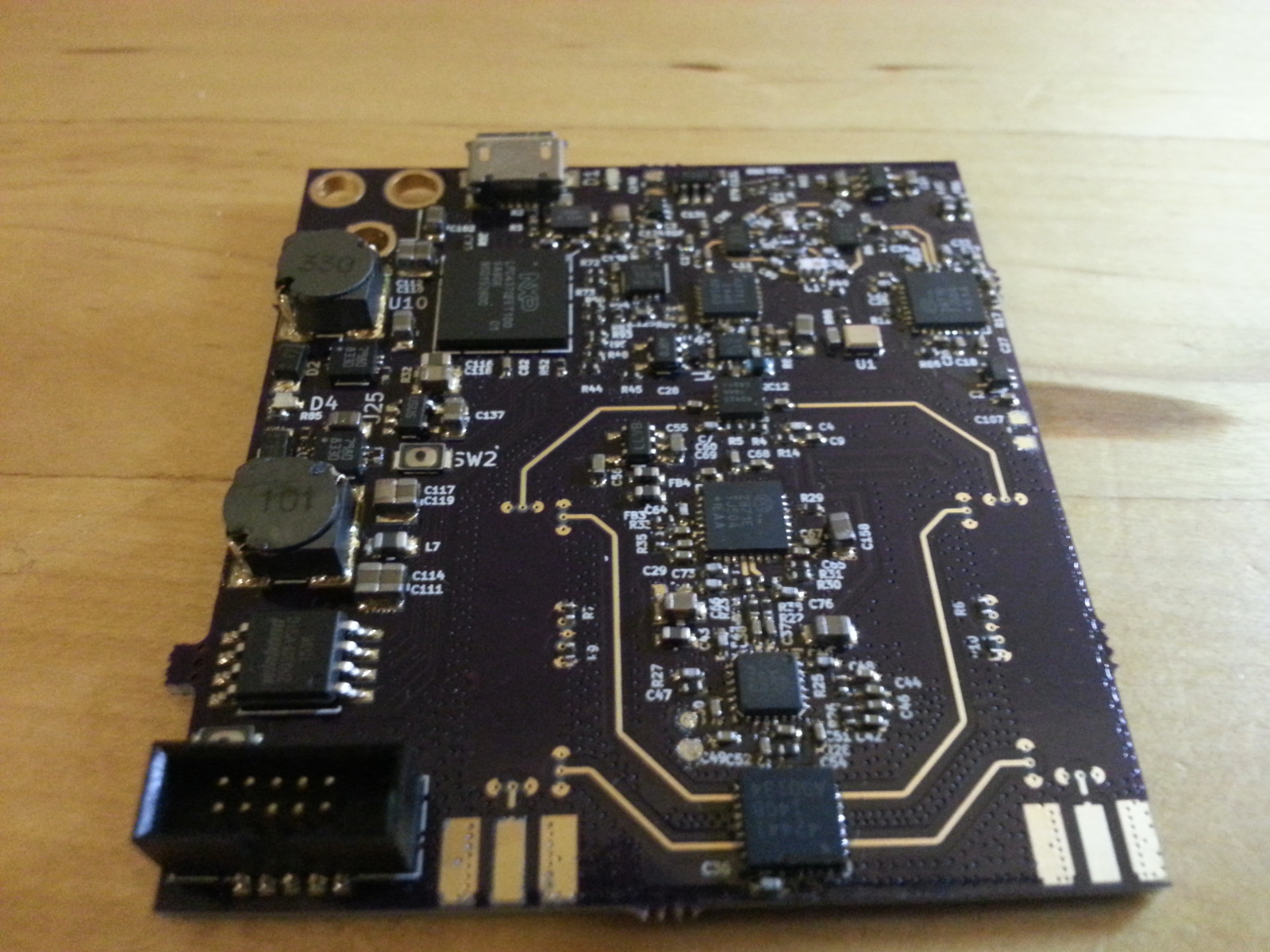
This PCB is a personal record in saving PCB area. Size of the PCB is 52 mm x 57 mm and it has over 300 components mounted on both sides. It could have been made even smaller if it wasn't for the big directional couplers. Stripline construction requires that layers above and below it are left empty wasting a lot of space.
Soldering
Fresh PCBs. Manufactured by OSH Park.
First I soldered the passive components on the backside.
Stencil on the top side. Stencil is made by OSH stencils
Solder paste spread on PCB.
Components placed by hand.
After few minutes in oven components have been soldered.
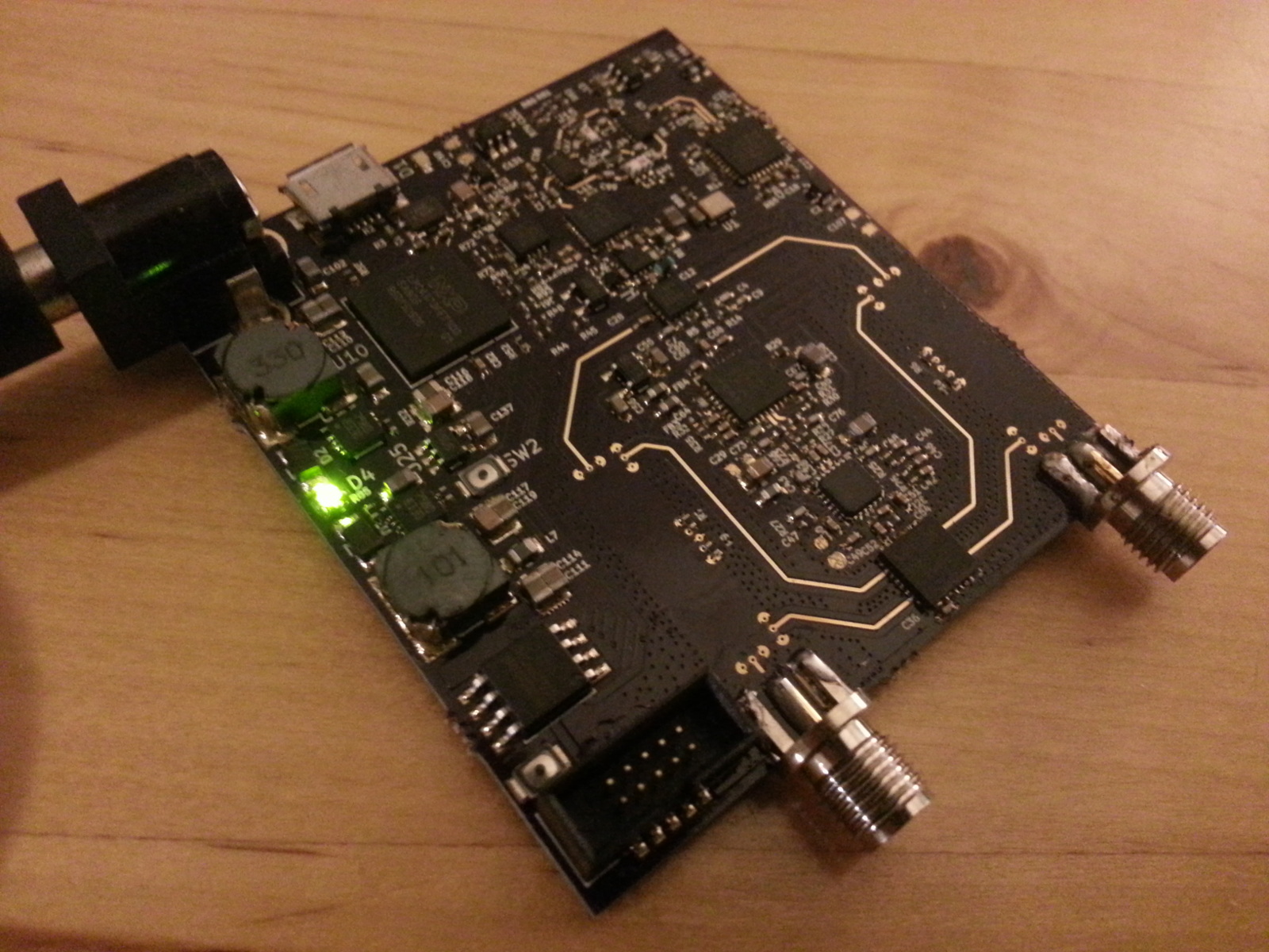
Connecting power for the first time.
On first power up everything seemed to work fine. Although I found out that I had made a mistake in switching regulator compensation network design and both supplies had about 0.1 V switching noise riding on them. After recalculating and correcting the component values everything seemed to work fine. I could program the microcontroller, turn on the PLLs and see the correct looking IF signal with oscilloscope on the mixer output. It was working fine for few days, but suddenly though I couldn't communicate with the microcontroller anymore. I suspected an issue with soldering and I tried to reball the BGA and resolder it but it didn't help. I could communicate with the microcontroller again, but it would get hot and randomly hang when communicating through USB. I didn't find any mistakes on the layout. I also tried to remove and reball BGA on evaluation board of the same microcontroller and it started to have similar symptoms so I was pretty sure that there was something wrong with my soldering. Or maybe with the Chinese BGA balls I was using?
Unfortunately I didn't manage to get the BGA resoldered correctly and after few tries the solder mask of the BGA footprint was looking pretty damaged from desolderings.
Ruined PCB after removing the components.
So after letting the board be for few months I managed to find motivation to make another one. I desoldered the most expensive components and made a new board. This time I managed messed up soldering of the LO PLL package. I had broken my soldering iron while desoldering some of the components earlier and using my old unregulated iron I managed to lift data input pad of the LO PLL while cleaning the solder from the pads. I managed to solder a 0.1 mm diameter jump wire to QFN pad and the board could still be used.
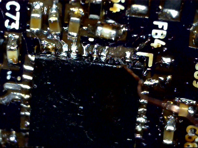
Jump wire soldered on the side of QFN.
Microcontroller still heated up more than seemed normal. It wouldn't run stable at full operating frequency, but after reducing the frequency from 204 MHz to 108 MHz it seemed to be working, although still running hot. I still couldn't find any issues on the layout though so maybe there is still some issues with soldering?
Signal processing
Firmware is based on the HackRF and AirSpy firmwares. Thanks to these open source software already implementing many of the features I needed, firmware development was much easier than if I would have neede to start from scratch.
In short, the sampling part of the firmware works by first setting the source and LO frequencies based on the commands from computer. RF outputs and amplifier are enabled, port switch, source filter and source attenuator are set to the correct values and receiver SP4T switch is set to the first channel.
Then computer sends a command to start sampling. DMA is configured to transfer 16k samples from ADC to memory and raise interrupt when done. As DMA moves samples in the background SP4T switch is switched so that every channel is sampled. When DMA complete interrupt is raised samples are sent to the computer. If more averaging is needed sampling is repeated and measurements are averaged.
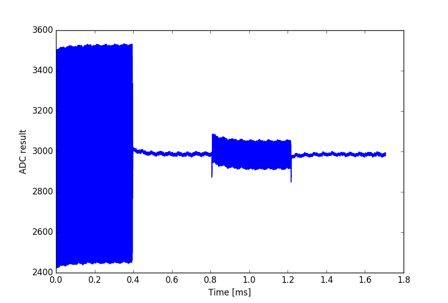
Samples on computer.
Computer program gets the recorded samples that look like in the plot above. In this case two port measurement is made so all four channels are sampled (In one port measurement sampling two channels is enough). First measurement is the port 2 reference channel RX2. Second is port 1 reflection channel A. Third is port 2 reflection B and fourth is port 1 reference RX1.
In this measurement we can see that source is connected to port 2 as port 1 channels RX1 and A only show leakage, while there is big signal on port 2 channels RX2 and B.
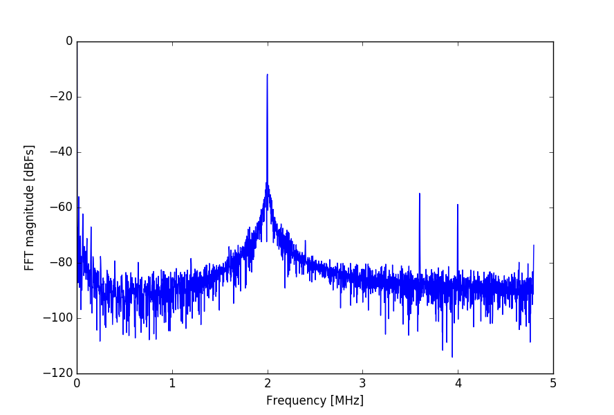
FFT of the RX2 channel samples.
Taking FFT of the RX2 channel samples reveals that the signal quality is quite good. ADC on the microcontroller also seems to perform surprisingly well. Y-axis units are in decibels full-scale, input sine wave with maximum amplitude without saturation would have an amplitude of 0 dB.
Signal level is -12 dB and noise floor near it is around -90 dB. Some noise can be seen near DC and bigger spurs at 3.6 and 4.0 MHz. High frequency spikes are likely result of mixer non-linearities. 4.0 MHz seems to be second harmonic of the IF signal, but I'm not sure where the 3.6 MHz comes from.
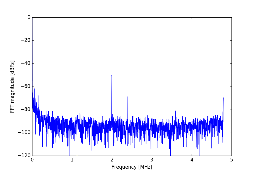
FFT of the A channel samples.
Taking FFT of the A receiver samples reveals that some signal is detected even though on the plot amplitude looks very low. Measured signal level is -50 dB full-scale. This time signals at 3.6 and 4.0 MHz have disappeared which makes sense if their level as mixer products is dependent on the signal level. However at 2.6 MHz there is a small spur. It can be seen on the first FFT too, although signal leaks little over it making it hard to see. Noise floor is at about -90 dB.
From the FFT plots magnitude and phase of the IF signal could be extracted, but there is no need to calculate all of the frequency bins when just one is needed.
\(k\)th frequency bin of discrete Fourier transform of signal \(x\) is defined as:
, where \(N\) is the length of the signal. We can use this definition to calculate coefficient of only one frequency bin. Time complexity is O(n) instead of O(n log(n)) of FFT, so in theory it should be faster.
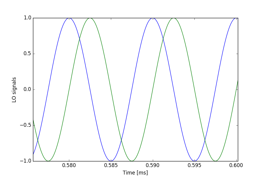
Generated digital second LO I and Q signals. In this plot frequency is lower than 2 MHz to make the shape more clear.
Two sine waves are generated at the signal frequency with phase difference of 90 degrees. Multiplying slices of the signal with samples from one channel and same index slices of two sine waves and taking separately averages of the results gives real and complex part of the IQ sample. Taking slice also of the LO signal is important for correct phase measurement. Absolute phases of the signals will vary as there isn't a reference channel to compare phase. However it isn't needed because S-parameters are defined as ratios of the measurements and relative phases are repeatable.
Next the port switch is switched and receivers are measured with source connected to the other port. After getting the IQ samples from all of the channels S-parameters can be calculated as ratios of calculated IQ sample of different receivers:
Superscript marks the port source is connected to.
We aren't however done yet. If we plot the S-parameters now we see that they don't look like they are supposed to. Reason is that there are many error sources in the measurements. Some of which are:
- Reflections from the components inside VNA and external cables.
- Directivity error from directional couplers.
- Leakage between the receiver channels.
- Attenuation and length of the cables and VNA internals.
Measuring the S-parameters of open circuit gives the following plots.
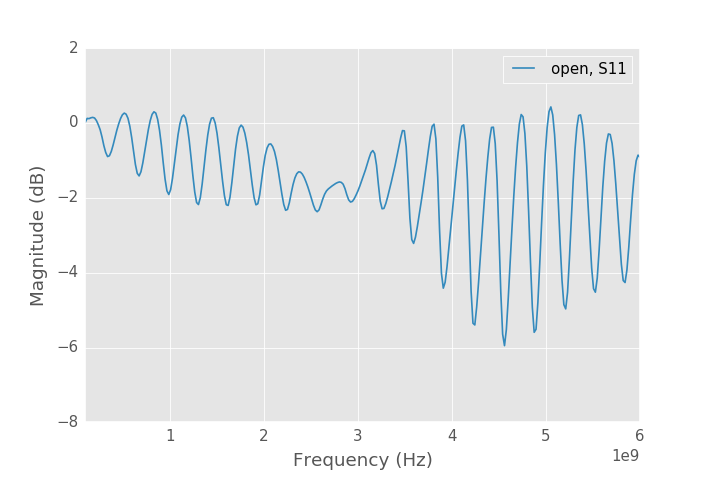
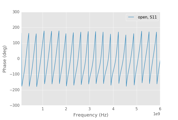
Ideally open circuit should have reflection coefficient of 0 dB and phase of the reflection should be 0 degrees.
To get accurate measurements errors must be characterized and mathematically removed from the measurements.
One port calibration
Calibrating one port measurements is much easier than two port as there are not as many error sources. Only one of the ports will be used and receivers on the second port are not measured at all. Result of the measurement is reflection coefficient of the device under test.
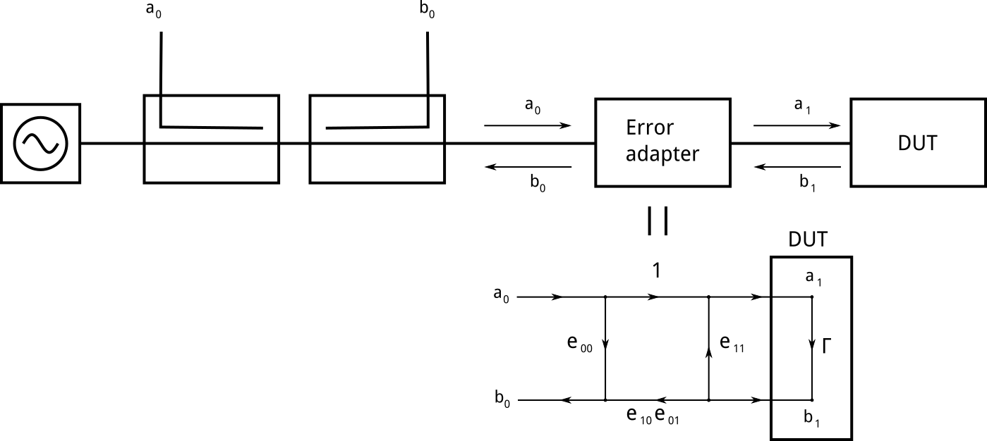
We can model the one-port VNA as an ideal VNA in series with error adapter. \(a_0\) and \(b_0\) are the measured RX1 and A channels. Measured reflection coefficient can be calculated simply as \(b_0/a_0\).
In the error adapter \(e_{00}\) term is the directivity error of the directional couplers. \(e_{11}\) includes errors from port matching and \(e_{10}e_{01}\) term is tracking error. It models different frequency responses of the detectors, for example phase error from cables is corrected by this term. \(\Gamma\) is the actual reflection coefficient of the device under test and what we want to measure.
For good overview of VNA calibration methods see this document and this page for more detailed explanations of the error terms.
Error adapter has three unknown terms so by measuring three known devices we can solve for the error terms. With the solved error terms we can solve for the actual reflection coefficient of the DUT.
The only problem is that three accurately known devices are needed. If the actual reflection coefficients are different from the ones used in calibration, there will be errors in the measurements.
Accurate calibration standards are really expensive as they require very high precision construction. At ebay professional calibration standards with SMA connectors sell for 300 € to 5000 €. Even the cheapest ones cost more than I have so far spent on this project.
Following the example of IN3OTD who made simple calibration standards, I decided to make calibration standard myself.
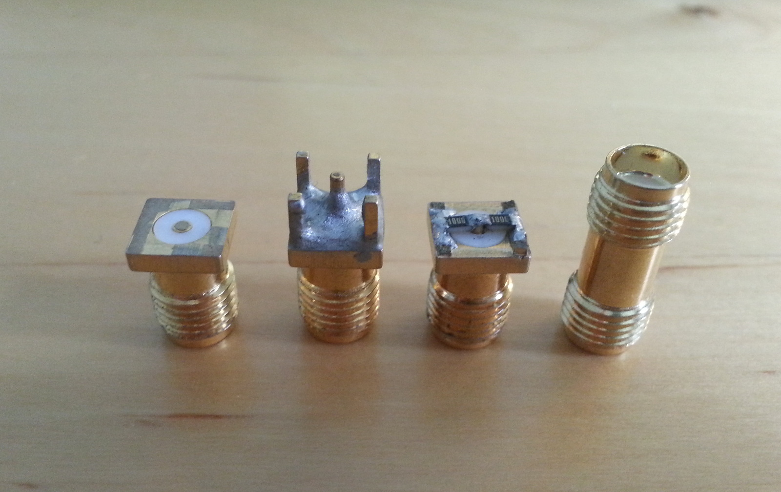
Homemade SMA calibration kit. Open, short, match and through standards.
I took three through hole SMA female connectors. Cut off legs from one to make open, one was filled with solder to make short and match was made by soldering two 0805 0.1% 100 ohm resistors in parallel to the last one. Through standard is needed for two port calibration and it is a regular SMA female-to-female adapter.
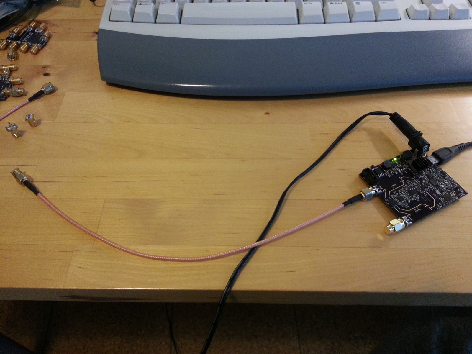
Measuring the calibration standards.
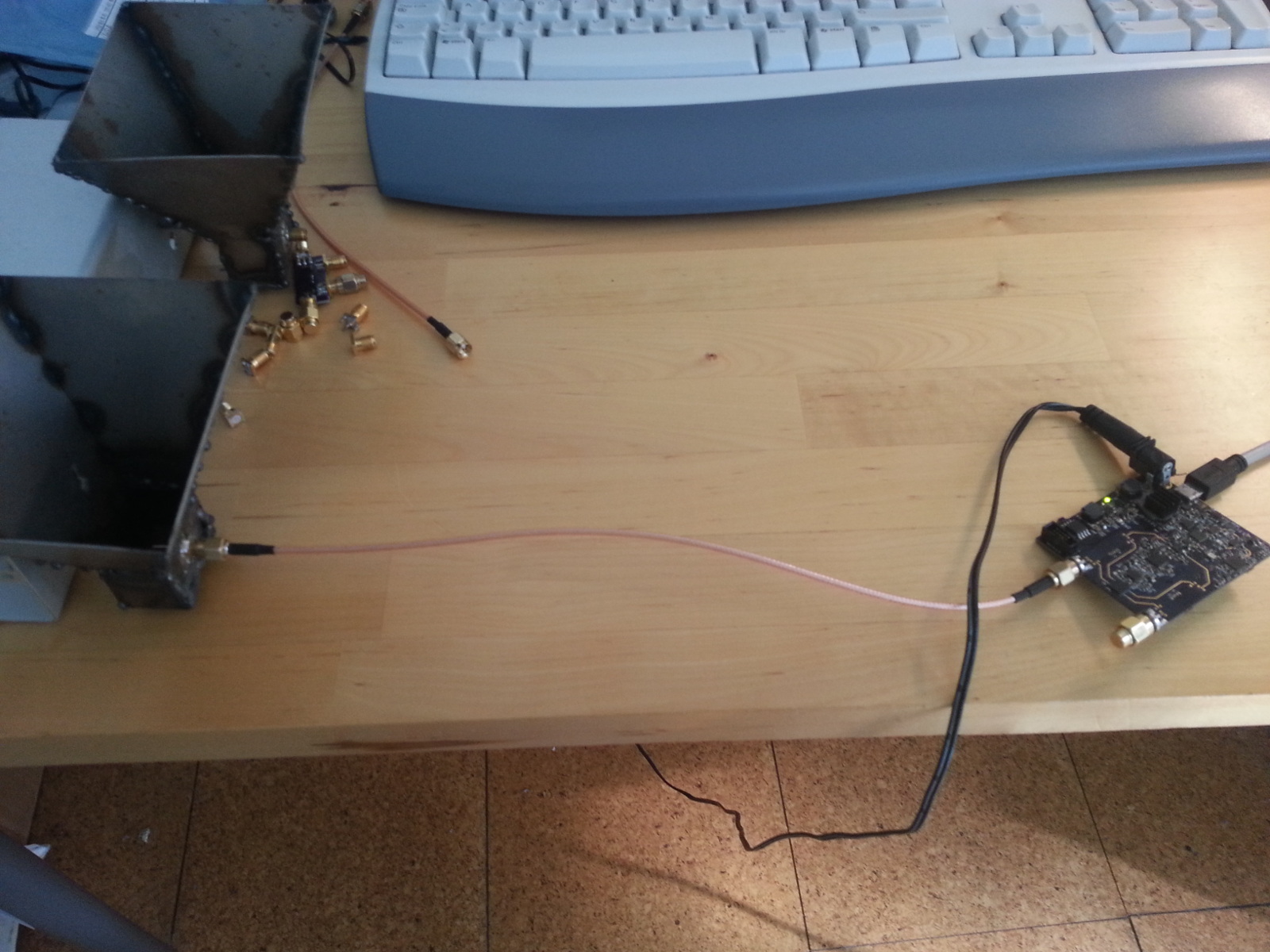
Measuring a horn antenna.
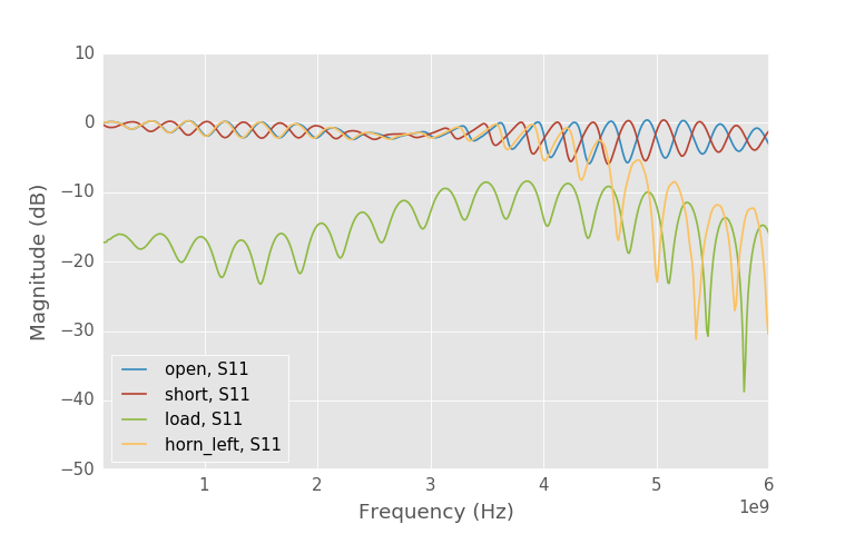
Uncalibrated responses of calibration standards and horn antenna.
In the above plot are the uncalibrated S-parameters of calibration standards and horn antenna. With little imagination it can be seen that horn antenna looks like open circuit at low frequencies and is well matched above 5 GHz. This plot also tells that internal errors are biggest between 4 and 5 GHz as the ripple there has largest magnitude.
Calibration is done using existing one port calibration routine in scikit-rf Python library.
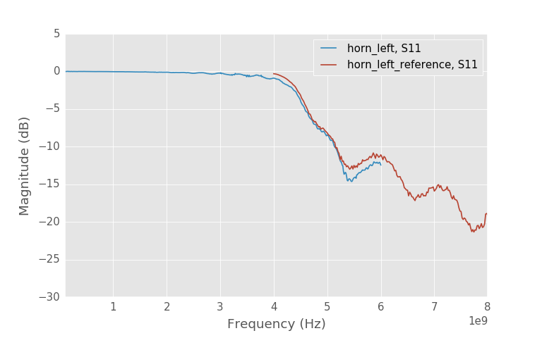
Input return loss of horn antenna measured with this VNA compared to measurements from professional grade VNA.
Above is the input return loss of horn antenna after calibration. Now the trace is much cleaner compared to the uncalibrated one. On blue is the return loss measured with this VNA and on red is same antenna measured using professional grade VNA made by Agilent. Exact model I used is now obsolete, but similar one would cost about 15,000€ as new. My VNA is able to make this measurement quite accurately considering the price difference. There are small differences in the plots, likely because of my inaccurate calibration standards.
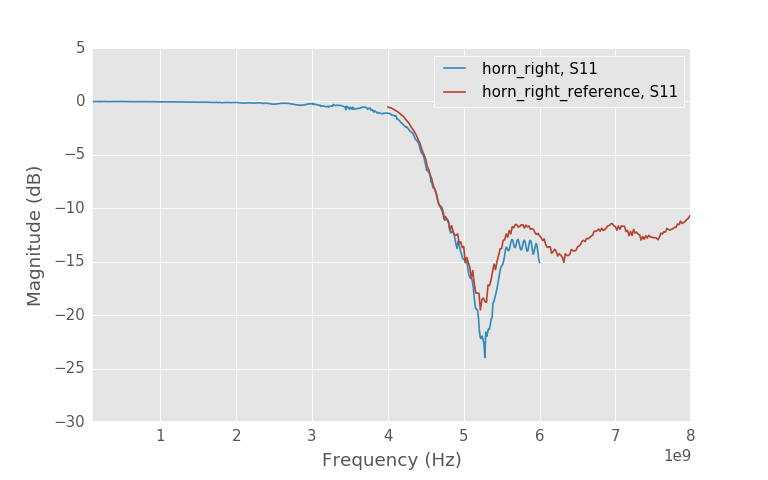
Return loss of the other horn antenna.
Other horn antenna measurement also agrees with the measurement made with Agilent's VNA.
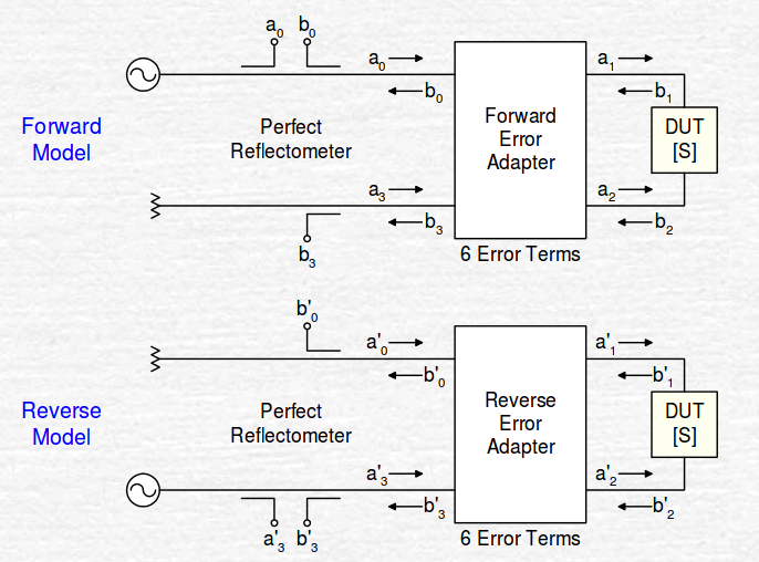
Two port calibration
Two port calibration is much more difficult than one port calibration because there is also additionally problem with calibrating the leakage away. Most commonly used error model is 12-term error model where both ports have 6 error terms, but this error model doesn't model leakage paths between different receivers and thus it can't remove errors caused by the leakage from the measurements.
12 term error model. Source
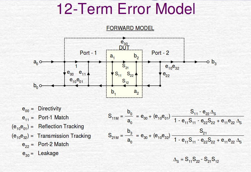
12 term error adapter parameters. Same model is used for the other port. Source
Calibration standards needed for this model are open, short, match and through. Open, short and match are measured at both ports one at a time and one port calibration is performed on both of the ports. Through measurement is used to calibrate the transmission from port to port. In the model there is a \(e_{30}\) term that models port to port leakage, this isn't however solved in the scikit-rf package I'm using to calibrate. It is often assumed to be zero as good VNAs have very high isolation between the ports.
Measuring 20 dB attenuator
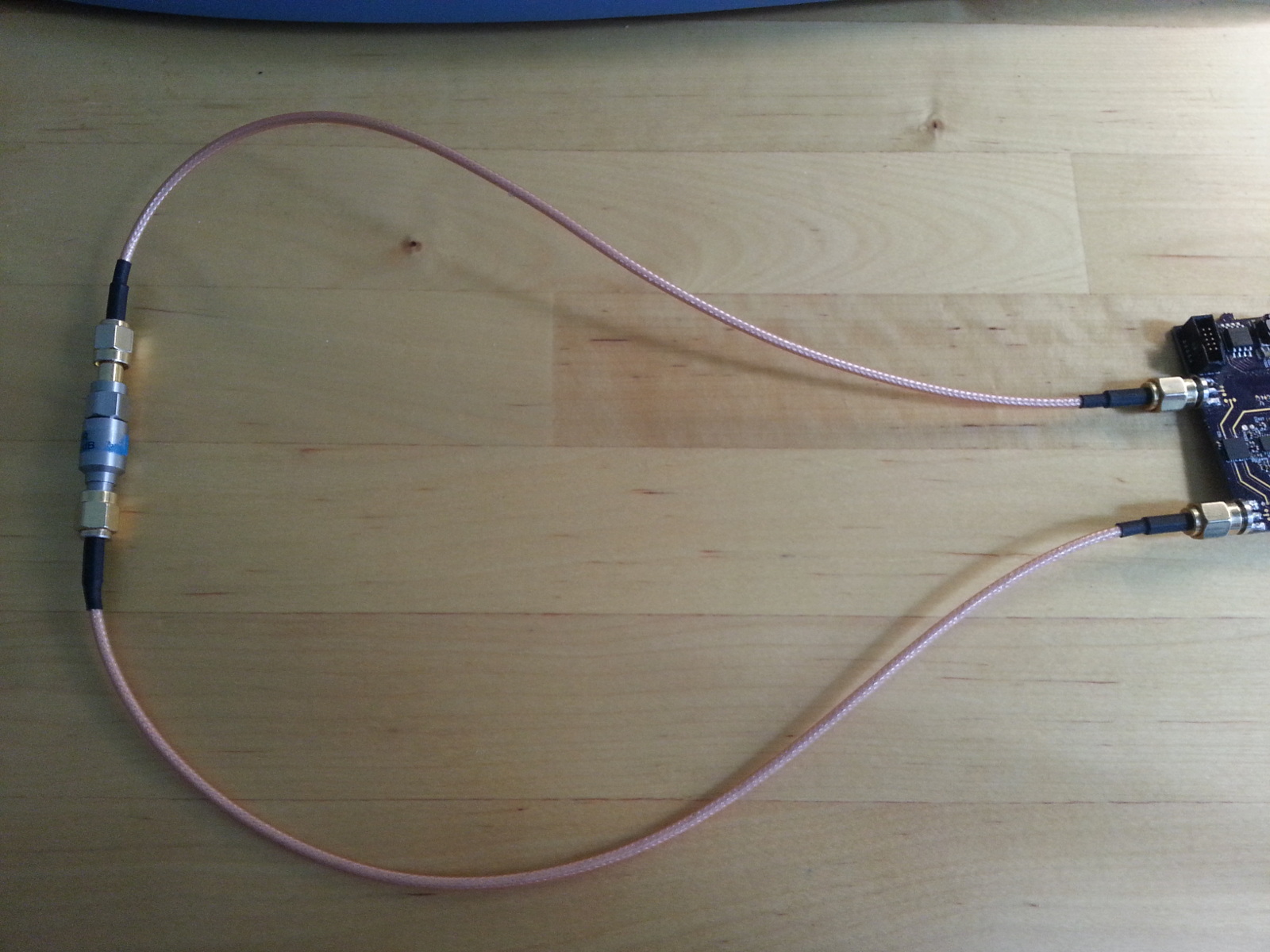
20 dB attenuator connected for measurement. Female-to-female SMA adapter is used on the male connector to connect to SMA cables.
To test the accuracy of 12 term SOLT (short, open, load, through) calibration I measured a 20 dB attenuator.
According to the seller this attenuator should have attenuation of 20 dB +- 2% and return loss better than -17 dB. However it is a cheap Chinese one so who knows what it really looks like?
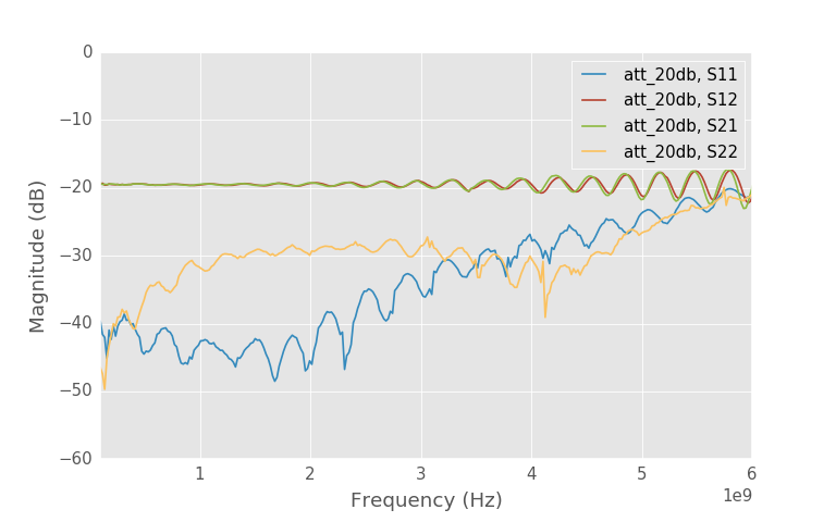
Above is the SOLT calibrated S-parameters of the attenuator. Matching seems to be very good and it seems to fulfill the -17 dB specification. At low frequencies measured attenuation is -19.5 dB which is just outside the promised 2% accuracy. Slight offset might be caused by inaccurate calibration standards. At low frequencies traces look okay, but at high frequencies there is weird ripple which is also seen in S11 and S22 measurements. I assume this is due to leakage which isn't corrected by this model.
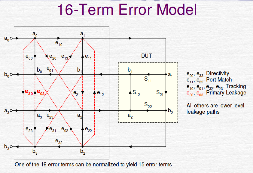
16 term error model. Source
To get more accurate measurements, error model is needed that takes into account the leakage terms between all of the receivers. 16-Term error model is a complete error model for two port VNA. It includes all the possible paths the signal can travel. Using this model on well isolated VNA causes more harm than benefit due to increased numerical errors if the real values of the leakage paths are below the measurement capability.
I decided to use a calibration method called LMR16. Due to increased number of unknowns in 16-term error model more measurements are needed. This method needs three different calibration standards: Through, match and reflect. Reflect can be any reflecting standard, match is assumed to be perfect and through is assumed to be lossless and well matched. Five different measurements are needed to get enough equations to solve for the unknown error terms:
- Through (Ports connected together with through standard)
- Match-Match (Match on both ports)
- Reflect-Reflect (Reflect on both ports)
- Reflect-Match (Reflect on port 1, match on port 2)
- Match-Reflect (Match on port 1, reflect on port 2)
LMR16 is a self-calibration procedure that can either determine the correct length of the through standard when reflect standard is given or the other way. This is convenient feature since I don't know the electrical length of the through, but short and open models are reasonable accurate according to the one port measurements.
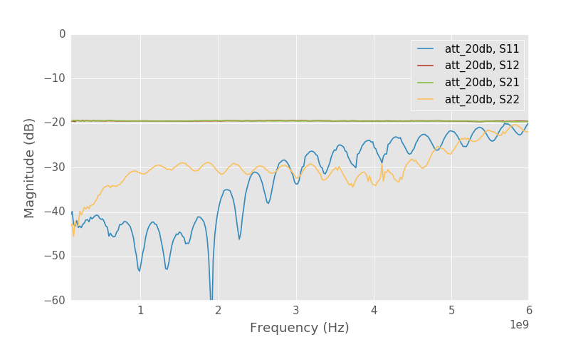
20 dB attenuator S-parameters with LMR16 calibration.
Above is the plot of the same 20 dB attenuator measurement, but this time calibrated using LMR16 calibration. Most of the ripple on the S21 and S12 plots has disappeared. Doing a secondary calibration using 12-Term SOLT further slightly improves the response as LMR16 assumes match standard to be perfect and SOLT calibration corrects for the non ideal match.
Response looks like it should. Insertion loss is very stable as a function of frequency and both ports are well matched. Some ripple is seen on S11 and S22 traces that looks like it shouldn't exists. Measured reflections are similar level as leakage so maybe there is some residual error left. I'm not sure why it exists, but some possible reasons I can think of are: inaccurate calibration standards and components heating up during the measurements and their parameters changing.
Solved through length is equal to 41.1 ps delay corresponding to about 8.7 mm long coaxial cable assuming that through material is PTFE.
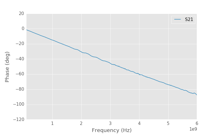
Measuring coupler
Coupler with SMA connectors.
To have something to measure I made a coupler board with SMA connectors. Coupler has four ports, but VNA only has two so I used SMA terminations on the two unused ports.
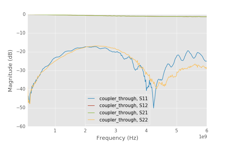
In above plot through path is measured with terminations on the coupled line outputs. SMA connector and coupler seem to be well matched. Return loss is better than -17 dB over the whole range.
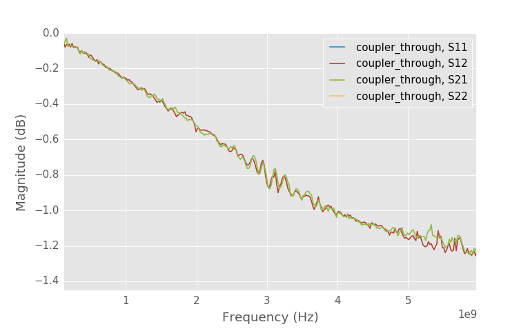
Close-up to the insertion loss.
Insertion loss of the coupler is also reasonable. About -1.3 dB at 6 GHz. Measured trace is also decent quality compared to the S21 trace with 12-term calibration. There is about 0.1 dB peak-to-peak ripple on it.
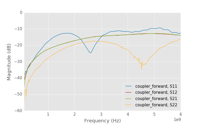
Measured forward coupling.
Next measurement is coupling in the forward direction. VNA was connected to the two rightmost ports while other two were terminated. Coupling at low frequencies is very low as was simulated. Peak coupling is -13 dB, when -15 dB was the simulated value.
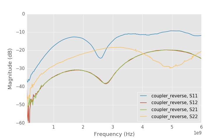
Measured reverse coupling.
Coupling in the reverse side however is higher than expected. It doesn't seem that the directivity is as good as simulated. Some of it is because termination on the through port causes reflections. It can be seen on the S11 that return loss is much higher than when through was measured indicating that termination isn't well matched. Better termination or mathematically compensating for it would be needed for more accurate measurement.
It is however possible that the directivity at high frequencies isn't as good as simulated when looking at the uncalibrated values. Amplitude ripple is highest between 4 and 5 GHz where directivity is low according to the measurements.
Conclusion
Looking at the uncalibrated values internal errors of the VNA seem to be quite big at higher frequencies. Sweet spot for minimum errors and good coupling seems to be around 2 - 3 GHz and at this range VNA gives the best accuracy. With correct calibration procedure the errors can be calibrated out and resulting measurement are quite high quality when cost of the board is considered. Performance seems to be good enough for non-professional use. Simple measurements such as antenna return loss measurements can be performed with high accuracy.
I'm not selling these, but if you are interested in making your own VNA or are just interested in looking at the design files all hardware, firmware and processing software is available at GitHub.