In my first post about my evolutionary circuits project I wrote about an evolved BJT inverter. I have since that post written some new features in the program. Now it can measure the current taken from logic input and the power supply, so the last best solution where the transistors would be fired shouldn't be possible anymore. I also made possible for the program to decide where the transition from high to low input should be. Last feature that I just finished a few minutes ago was constraints on the measured values. If measurements don't fill the constraints the circuit gets ranked very poorly and has a low probability to be chosen to the next generation. Reason I added the constraints was because I tried to evolve a BJT inverter before adding them and the program got stuck on the minimum where the best inverters low to high transition was very fast, but other transition didn't work at all.
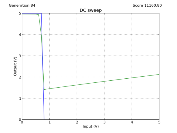
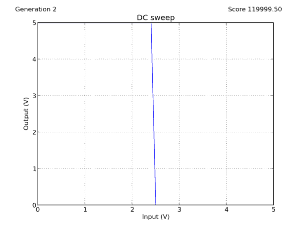
DC sweep of the broken inverter. Blue is the goal and green is the circuits output. With the 5V input output is 2.1V, which is above the transition voltage. If this inverter would drive another inverter the second inverter would output 1.5V which is the low voltage, but output should be 5V, same as input, because it was inverted twice.
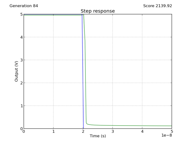
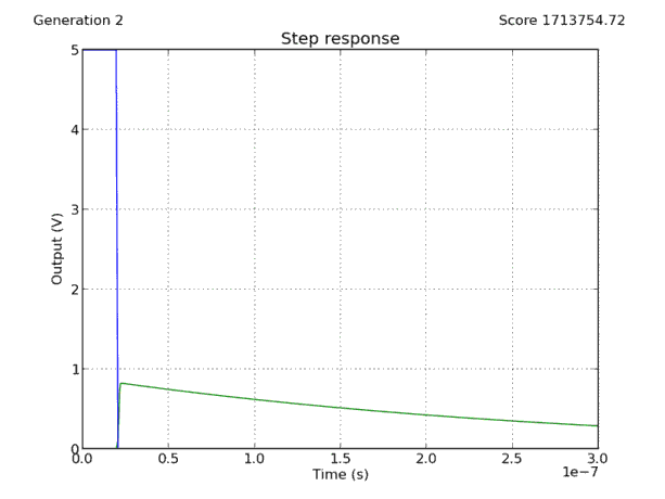
High to low transition is fast...
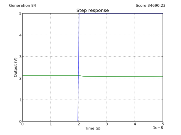
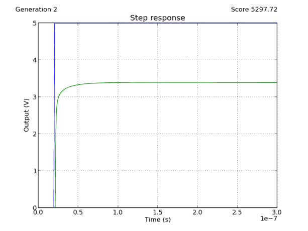
...But low to high transition doesn't work
So the constraints were necessary to guarantee that the program wouldn't get stuck on broken solutions. After implementing them I tried to evolve a BJT inverter again. Allowed components were: resistors, capacitors, 2N3904 and 2N3906 transistors. To avoid unreasonable big capacitors I limited the maximum capacitor value to 100pF. Picofarad capacitors were chosen because they are reasonable size for integrated circuits. Maximum number of components was 8 and population size was set to 4000 circuits. I also tried to model the finite impedance of the input with 50 series resistance and to avoid circuits that wouldn't work with load I fixed a 10kΩ load resistor to the output.
This time I measured: current taken from logic input, current taken from the 5V power supply, input DC sweep from 0V to 5V, high to low and low to high transitions. Because measurements from SPICE are in basic SI units, the program will rank 1A average decrease in current usage same as 1V average decrease in transfer curve, to get the program appreciate current more the current scores were multiplied with one thousand so that 1mA decrease in current would equal 1V decrease in the transfer curve.
Previously I arbitrarily chose the transition voltage to be 2.5V, but since then I have improved the program and now it's possible for it to decide where the optimal transition is. Ordinary RTL or TTL inverters don't switch exactly at the half of power supply value either and it's very likely that the evolved inverter would perform better if it wasn't artificially limited to switch at 2.5V.
Constraints were placed on the transient simulation values and DC current usage. After the transition the inverter was required to settle to 0.2V below or above the transition voltage depending on the which transition it was. This way the broken inverters like on the above hopefully wouldn't be possible anymore.
This time I ran the simulation a lot longer than in my first post. I started it in the morning before going to the work and stopped it after coming home. Total running time was 12.5 hours. Below are the animated gifs of the measurements of the best circuits of each generation, currents aren't plotted because they were so close to zero that they all looked just like a straight line. But if you still want to look at some straight lines here's input current and here is current taken from the power supply.
DC sweep. Blue line is the goal and green is the circuits output.
High to low transition. Scale of x-axis is 50ns/division.
Low to high transition.
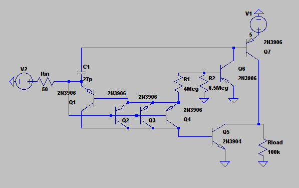
Schematic of the final circuit
Static current usage
Voltage supply V2 is the logic input and V1 is 5V power supply. This is very neat looking circuit, looks almost like it could have been designed by a human. It doesn't have any unconnected or unneeded components, even the 27pF capacitor is needed(It improves the propagation delay). Especially the input stage is interesting with the 3 parallel PNP transistors. Connecting transistors in parallel improves their frequency response and current handling capacity. If this is built from discrete components connecting transistors in parallel might be problematic because the transistor might not be matched that well. But it shouldn't be a too much trouble because single transistors could handle all the current going through the three of them. If this was an integrated circuit the 3 individual transistors could be combined to one three times bigger transistor.
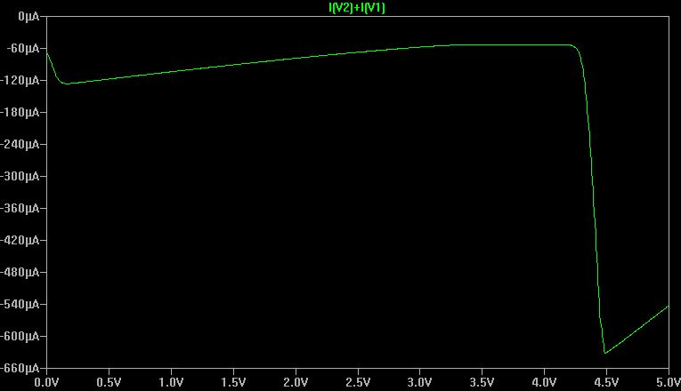
If you look at the above transient responses it looks like it's rise and fall time is really fast. In SPICE simulation both rise and fall time are about 1.3ns. If you compare these to the ordinary RTL inverter built with 2N3904 transistor and using 15k base resistors it has a fall time of 80ns and a rise time of almost 2µs(=2000ns). RTL inverters maximum static current usage is 1.5mA when input is at 5V. The evolved inverters maximum current use is just 660µA when the input is at 4.5V. Downside of course is that the evolved inverter uses more components than the RTL inverter.
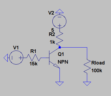
Schematic of RTL inverter
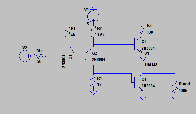
Schematic of one TTL inverter. This is commonly called a TTL inverter with a totem pole output stage.
But RTL is old technology and not in use anymore, but other bjt based logic family that is still used is TTL. When built with 2N3904 transistors the TTl inverters maximum static current consumption is 36mA. TTl inverter is quicker than the RTL inverter. It has a fall time of 1.8ns and a rise time of 1.6µs. The reason both RTL and TTL inverters have slow rise time is because after being in saturation it takes time to remove the stored charge from the base and get transistor to the cutoff state. Evolved circuit takes care of this by dumping huge current spike through the base of Q5. When the input changes state from 5V to 0V, it creates a current through the capacitor. Part of the current goes to logic input and part of it goes through the 4 PNP transistors at the input to the base of Q5. Voltage at the base quickly decreases to -2V. Size of the current spike depends on the fall time of the logic input. Quicker it falls the bigger the spike and faster the outputs transition is. It should be noted that even tough the maximum current in the evolved circuit is bigger than in TTL inverter its duration is very short and the total amount of energy required to change output is smaller in the evolved circuit.
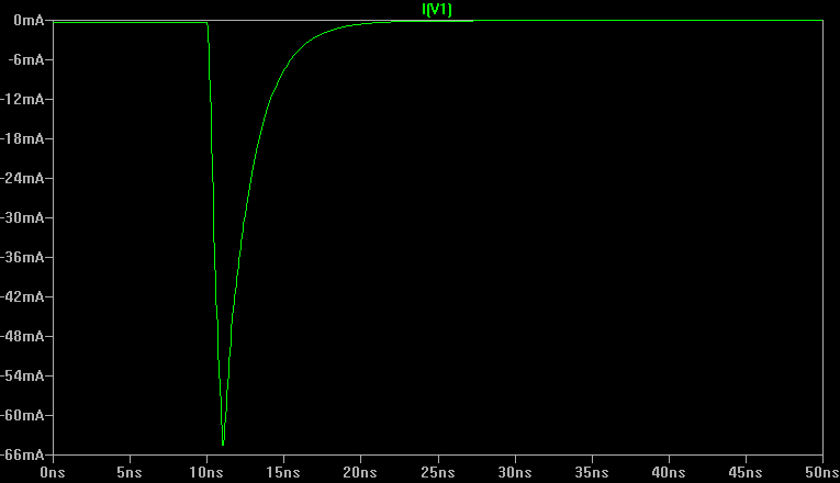
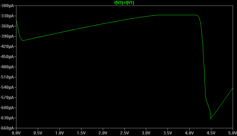
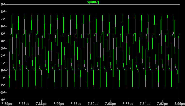
Current taken from the power supply. Input changes at 10ns. And it falls in 1ns. With 0.1ns fall time maximum current is 77mA. 2N3906 can handle 200mA of continuous current and even higher amounts for short time so this isn't enough to break it. 24mA of this goes through the Q5 and rest of it goes to logic input, which might be a problem for the circuit driving the inverter.
I also built the circuit to make sure that it works when built with real components. Unfortunately I have only single probe on my oscilloscope so I can't measure the rise and fall times and even if I had the second probe it would be a waste of time trying to measure this when built on a breadboard because breadboard has big parasitic capacitances which would mess up the capacitances near the 10pF capacitor. So this should be built on either IC or using the Dead bug style. But I could measure the static current usage and the input DC sweep:
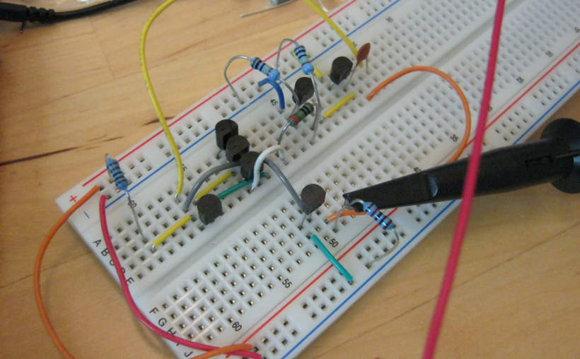
Built with real transistors.
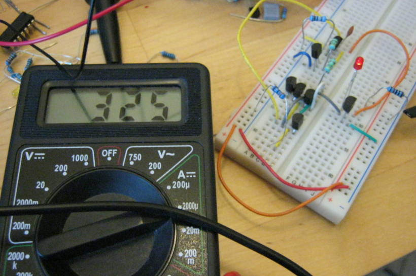
Current when the input is at 0V. 325µA. You can also see the LED at the output light up.
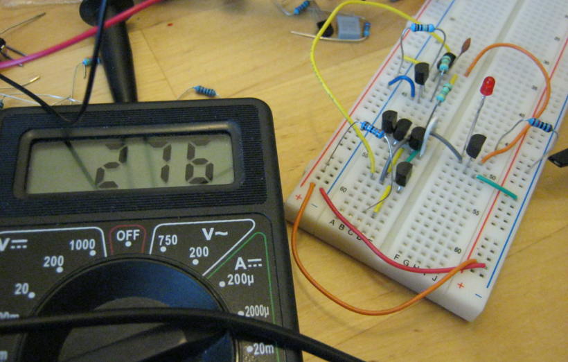
Current when the input is at 5V. 276µA. 0V on the output as you can see from the LED.
Simulated with LED and 10k resistor at the output.
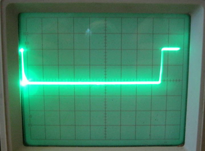
DC sweep with triangle wave at the input. 0V is at the left and 5V at the right. Transition voltage is about 4.5V as simulated.
Current is near the simulated values but not quite there. 0V input current is very near the simulated value but the 5V input for some reason is much less. No idea whats going on here. Tolerances on the transistors or resistors?
Could this circuit be used in a production? Maybe, even though it has some problems it's faster than the ordinary TTL inverter. It has a few problems with the big resistor values, small 27pF capacitor and current spikes in the logic input and the power supply. It also has a few volts of overshoot on the output voltage on high switching frequencies. Replacing the Megaohm resistors with smaller values helps but increases current usage.
Overshoot on the output. 33MHz switching frequency. Faster than the TTL inverter is capable of(when using 2N3904 transistors, it can go higher with faster transistors. Same with this circuit).
When fast rise and fall time is important this might be useful circuit, but before using it anywhere it might need some hand designing to fix the overshoot and current spikes. Overall it is a big increase in the quality compared to the previous inverter circuits.
If you want to try it yourself download the code from github and run the "inverter.py" file. That version also has scoring for the transient current usage. The program works on Linux and might or might not work on Windows.