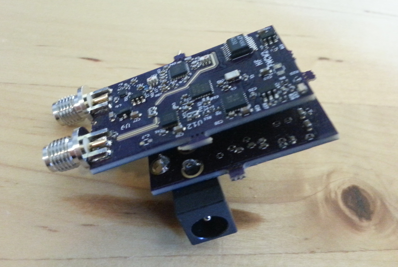
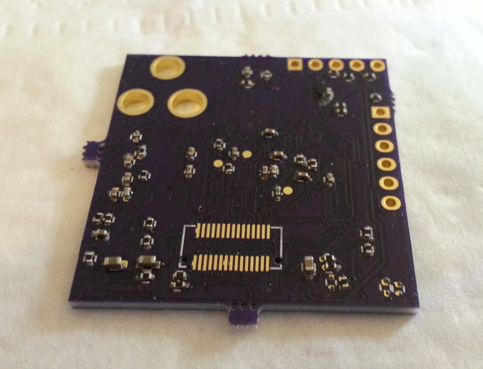
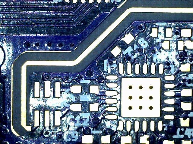
Finished radar boards without antennas.
Introduction
Previously I made a very simple frequency-modulated continuous-wave (FMCW) radar that was able to detect distance of a human sized object to 100 m. It worked, but as it was made with minimal budget there was a lot of room for improvement.
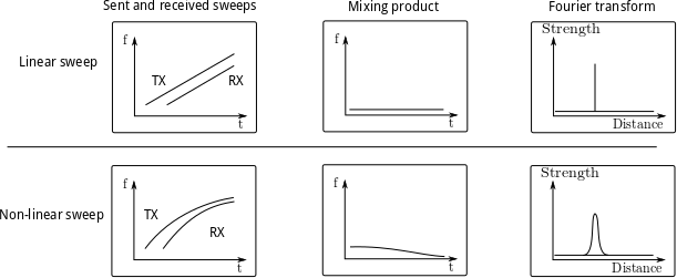
Non-linear frequency sweep causes decreased resolution.
One of the bigger problems was that voltage controlled oscillator (VCO) generating the high frequency output signal was driven directly from the digital-to-analog converter (DAC) of the microcontroller. VCO tuning voltage and output frequency relation is not linear and using a linear ramp as a tuning voltage generates slightly non-linear frequency sweep. If the frequency sweep is not linear it generates non-constant mixing tone at the baseband. FMCW radars use Fourier transform of the baseband signal to find the distance to the target and when the received tone is not constant it spreads the power in the frequency domain and target resolving resolution decreases.
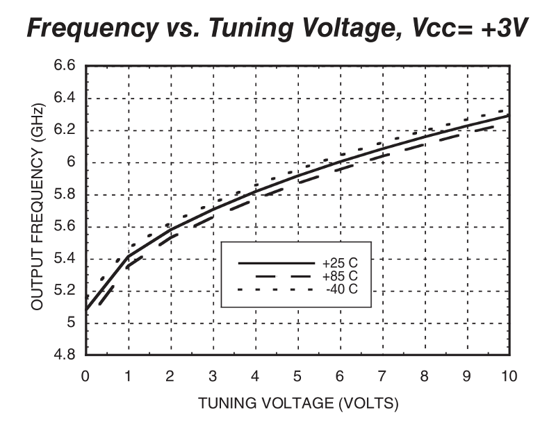
VCO's output frequency as a function of the tuning voltage. Ideally this would be linear.
A linear sweep can be generated by pre-distorting the VCO tuning voltage so that result is a linear sweep. Drawback of this method is that it requires knowing the exact VCO voltage/frequency characteristics which varies to some degree as a function of temperature and from component to component. Other way is to use a phase locked loop (PLL) that uses a frequency divider to measure generated RF frequency and compares it to accurate low frequency reference oscillator. A feedback loop then adjusts VCO tuning voltage so that divided frequency equals the reference oscillator frequency, this forces the RF signal frequency to be division amount times the reference oscillator frequency. Sweeping the divider value in small fractional steps can be used to generate a very linear sweep. Alternatively reference oscillator frequency can be swept while keeping the divider constant.
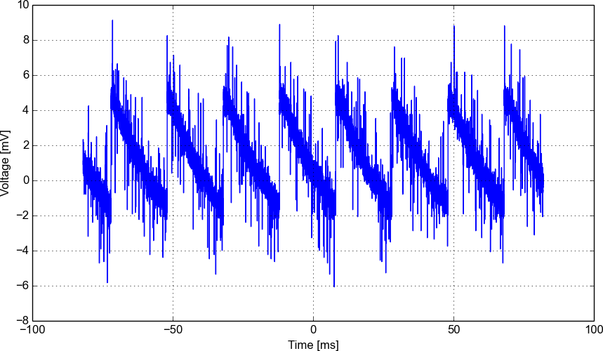
Mixer output of the old radar when antennas are replaced with loads. Waveform is caused by the LO leaking to RF input port of the mixer.
Receiver also had few problems. First being that baseband low frequency amplifier just didn't have enough gain to amplify low power echoes from far away limiting the maximum range. Other receiver problem was DC mixing product changing during the sweep and creating AC signal.
Receiver LNA had a gain of 13 dB and mixer after it had a conversion loss of 8.5 dB. This only leaves 4.5 dB of gain at RF section and causes the baseband low frequency signals to have very low amplitude. Since the receiver is a direct conversion receiver, LO oscillator leaking to RF input port of the mixer is going to cause a mixing product at DC. Power amplifier output power and mixer conversion gain vary with frequency causing the DC offset term to also vary. It creates an AC signal with frequency equal to sweep repetition frequency. This frequency is around 1 kHz and is amplified by the baseband amplifier. Since RF gain is low, this leakage signal can have bigger amplitude than the received signal saturating the baseband amplifier. A better mixer with more isolation, PA with less gain variation, more gain at RF and high-pass filter after mixer can be used to minimize this effect.
Last problem was with the microcontroller. It was not fast enough to transfer all the ADC samples to PC through USB. It was able to transfer only 25 sweeps/second while radar would take 500 sweeps/second. It probably would have been possible to improve firmware but strict timing constraint for generating the VCO ramp signal would had made it hard.
Because of the various problems with the old design I decided to make a new radar that fixed the problems.
New radar
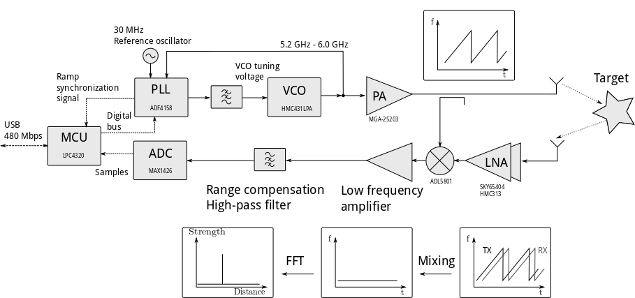
Block diagram of the new design.
The new radar design is very similar to the old one on system level, but with few improvements. It functions using same principle: Transmitted linear sweep reflects from target and is received at the receiver. There it is multiplied with copy of transmitted sweep. Since electromagnetic radiation travels at speed of light, there is a time difference between received reflection and transmitted sweep. Multiplication in mixer generates a low frequency signal that has a frequency proportional to travel time of signal. Fourier transforming the mixer output signal gives frequencies in the signal and it can be used to resolve more than one target at the same time.
Biggest difference is addition of PLL that linearizes the transmitted sweep. PLL used is ADF4158, it is designed especially for radars and it can be programmed to generate accurate sawtooth and triangular ramps.
Other changes include: much faster microcontroller, better receiver, better baseband filtering and various other small improvements.
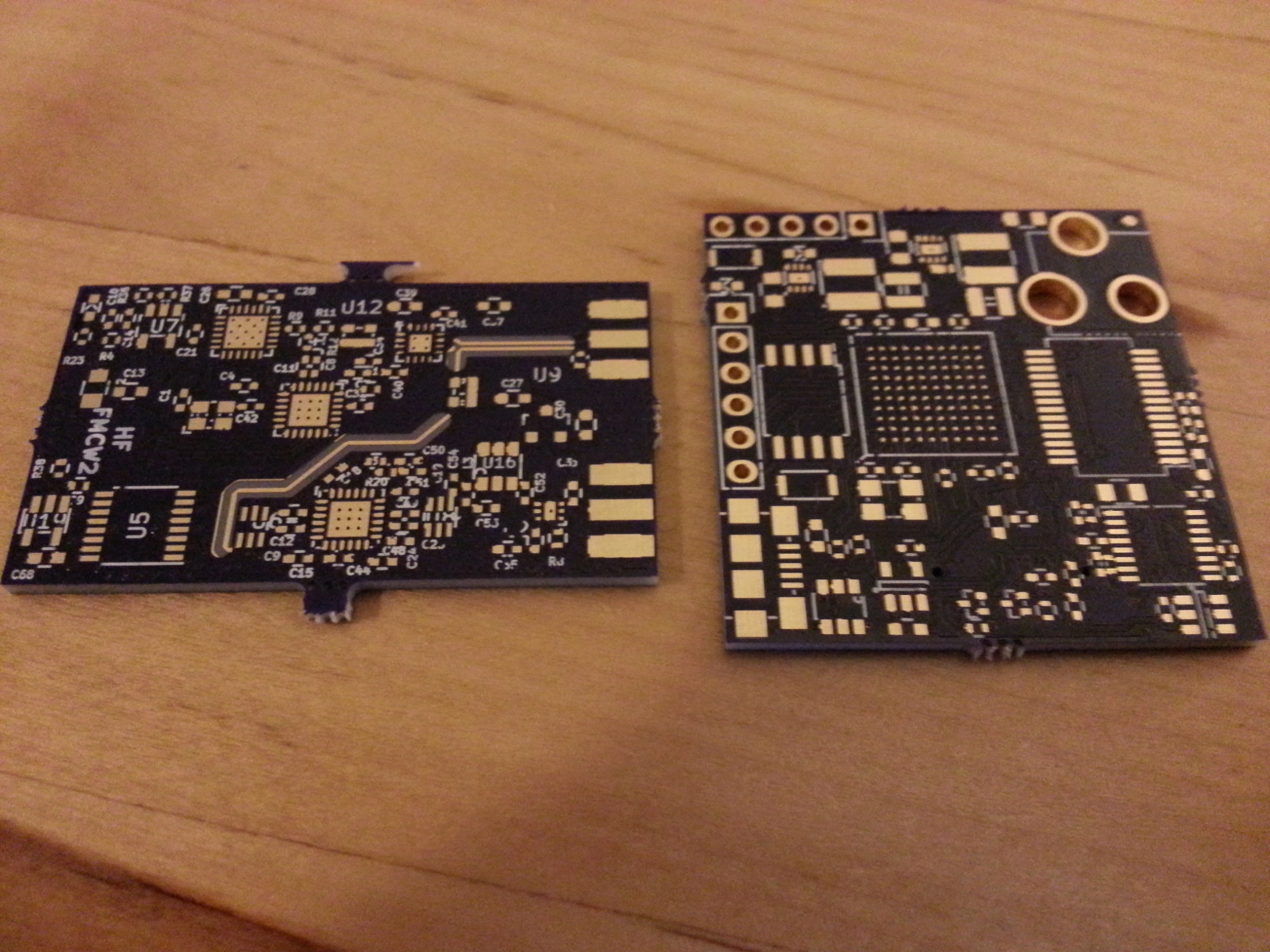
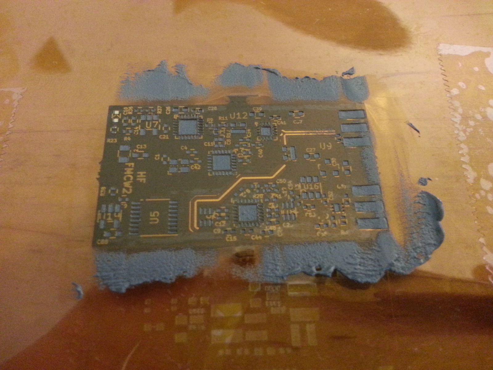
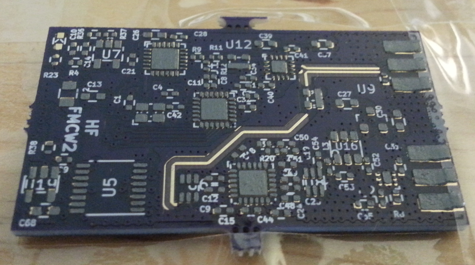
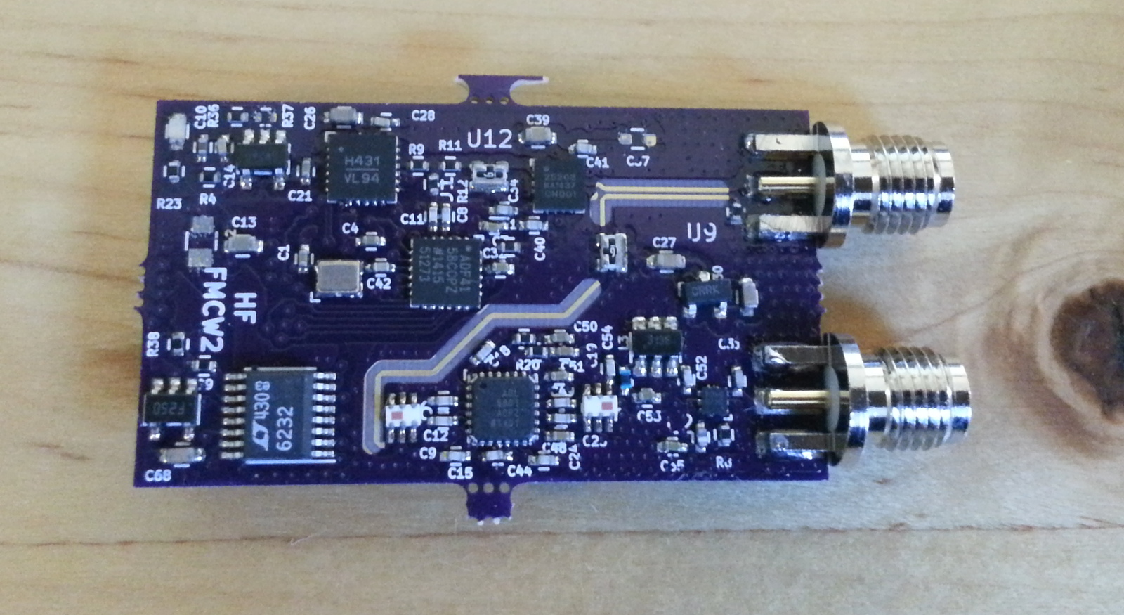
Bare PCBs.
Design is split it two boards. One has digital functions and other high frequency parts. One of the reasons was that if I made a mistake with the PCBs, with two board design I could probably only order one new board and save money. Two boards also reduce the noise going from digital board to RF board.
RF board needs to be four layered, because 50 ohm transmission lines would be too wide on 2 layer board because of thicker substrate. Four layer board is also made out of better material with lower loss and more stable parameters. Digital board could be made with two layers to save money as four layer board costs two times as much as two layer board for same area.
But it turns out that two layer board would need to be bigger as compact BGA components can't be routed on two layer board and bigger QFP packaged microcontroller would be needed. QFP takes more than four times as much area as BGA, so using BGA on four layer board turns out to be cheaper. It also enables packing the other components closer and results in better routing with less interference due to having more layers available.
Digital board
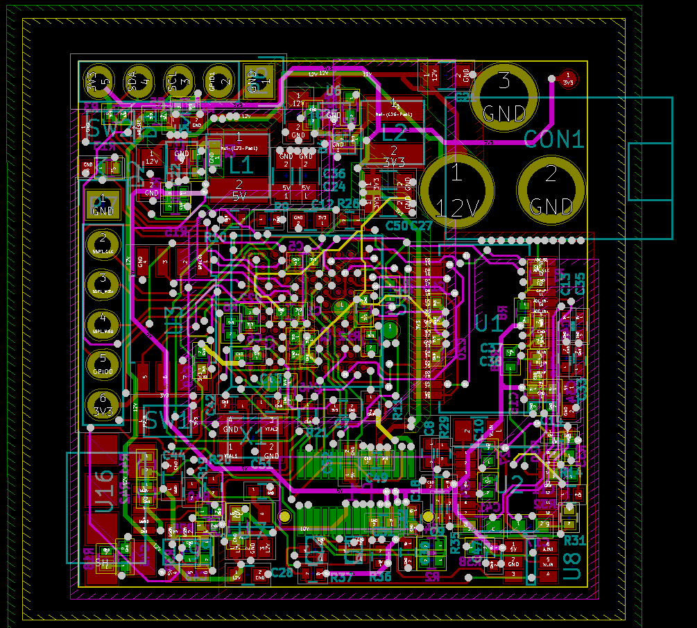
First I was thinking of having FPGA for signal processing, but they are expensive and don't have easy and cheap way to add high-speed USB communication. I ended up using NXP LPC4320 204 MHz ARM microcontroller. It has interesting serial GPIO (SGPIO) device that has several shift registers that can be configured very extensively. SGPIO can be used to implement communication protocols such as UART and SPI, generate PWM signals, interface to parallel output ADC which I'm using it for and various other things. SGPIO subsystem can be clocked up to 102 MHz allowing for very fast data transfer from ADC. Microcontroller also has high-speed (480 Mbit/s) USB, so this time the transfer rate shouldn't be a problem. It's also one of the cheapest microcontrollers with high-speed USB costing 7.2 € at low quantities at Digi-Key.
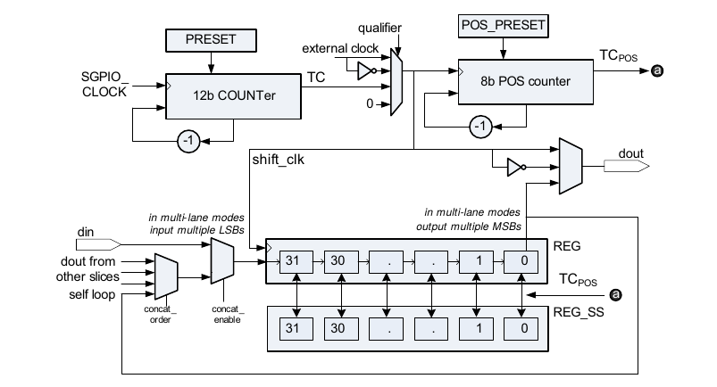
SGPIO slice block diagram. One slice can be configured as input or output, generate interrupts and clock source can also be configured. Slices can also output to other slices.
HackRF uses the same microcontroller for same reasons. Since HackRF is open source I'm able to use its software with small modifications. Existing software really helps especially as I don't have debug connector on board making it hard to see what the microcontroller is doing.
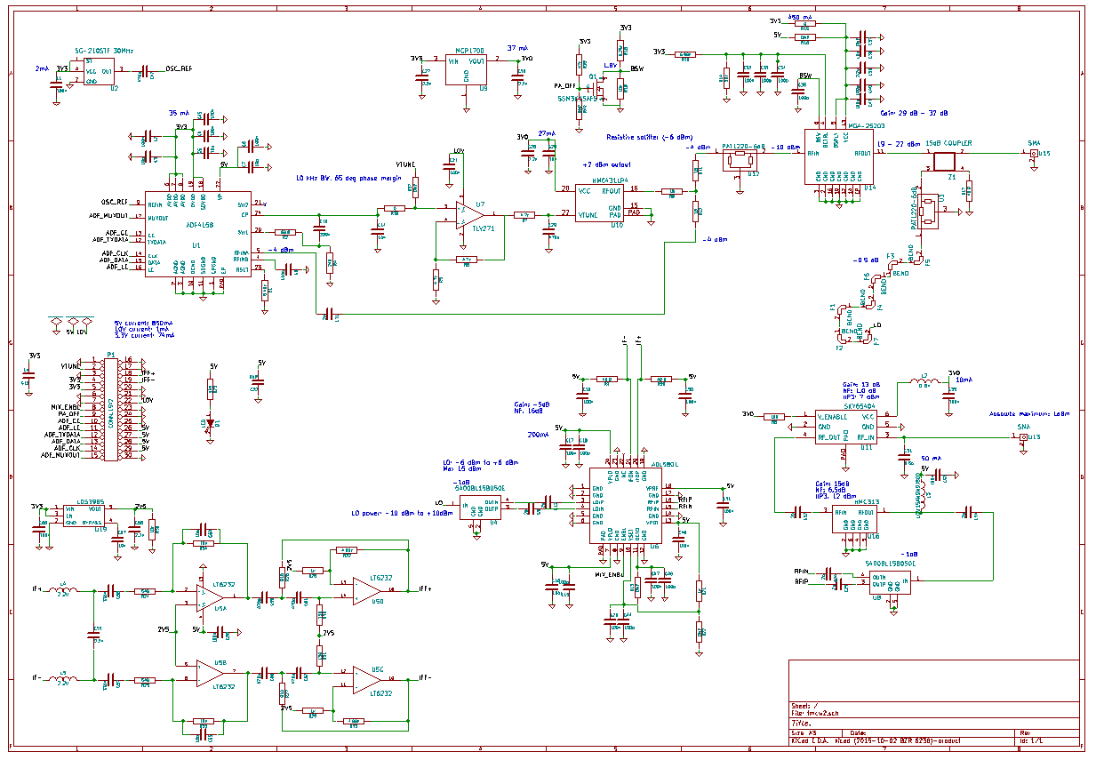
RF board
RF board is based on the ADF4158 PLL chip. It takes a 30 MHz reference clock and RF output from VCO as inputs. VCO output frequency is divided by programmable divider on the chip and divided frequency is compared to reference clock. Chip then outputs analog voltage to VCO's tuning pin to makes the divided RF frequency equal to reference clock. Since low frequency reference clock and divider can be made very accurate and stable, PLL chip makes the VCO output frequency to also be very accurate.
This chip is made especially for radar applications. Its divider value can be fractional so that RF frequency can be stepped in smaller steps than multiplies of the reference clock frequency. It also has internal function that can automatically step the divider value so that it generates linear sweeps ideal for radar without needing constant control from the microcontroller.
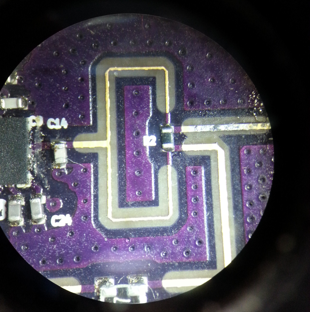
Mixer LO coupler. A small portion of the power amplifier output is coupler to mixer. Small footprint on right side is for 50 ohm resistor terminating the other branch of the coupler.
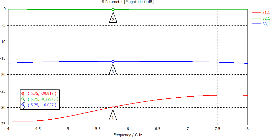
Coupler simulated S-parameters. S11 = input from PA, S31 = Coupler power to mixer and S21 = Power passed to antenna.
Previous radar used passive mixer with high local oscillator power requirement. Wilkinson divider after the PA was used to divide output power equally to antenna and mixer. Mixer wouldn't have needed that much power and it caused reduced efficiency and lower radiated power.
New coupler couples much less power to the mixer (-16 dB = 3%) and much more is passed to the antenna. Simulated power loss from power amplifier to antenna connector is only 0.23 dB (5%).
Reason for using sharp 90 degree bends with part of the corner cut off is that these corners are designed to minimize reflections of the bend. These kinds of corners are called mitered bends. Large diameter smooth bends could also have been used, but they take more space. Mitered bends are also used on the long trace to mixer local oscillator input.
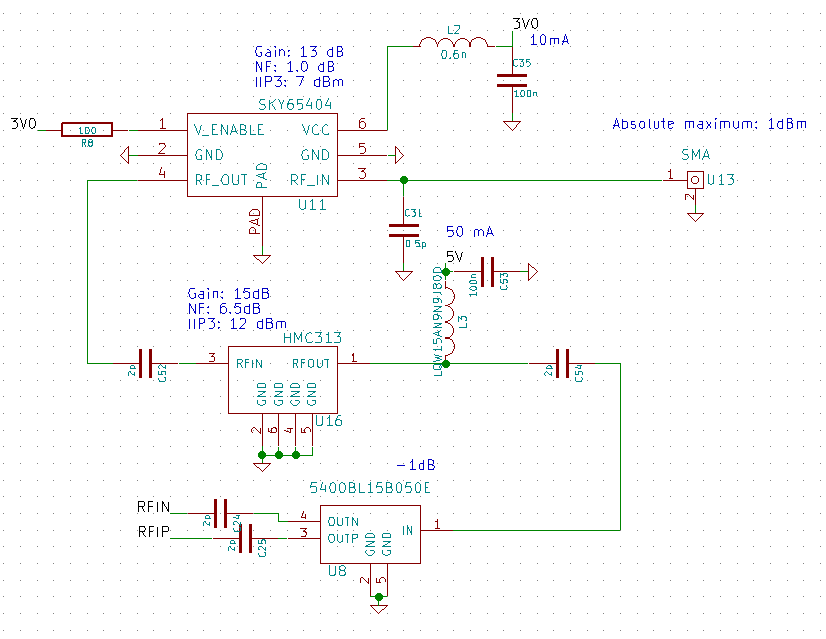
Low noise amplifiers. Receiving antenna SMA-connector on the top right, balun and mixer input at the bottom.
This time there is additional amplifier after the LNA to increase the gain before the mixer. Active mixer I'm using has a higher noise figure requiring more gain than the previous passive mixer to achieve low system noise figure. Noise figure of the system can be calculated using Friis formula. If only the first LNA would have been used noise figure of the system would have been 6 dB. With two LNAs noise figure is 2 dB.
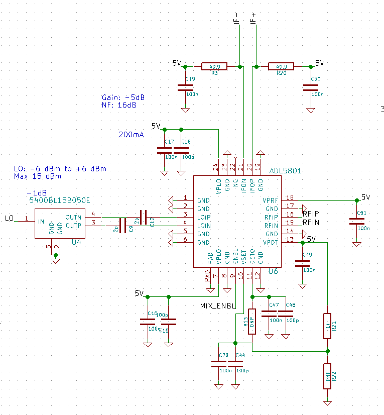
ADL5801 active mixer.
Instead of passive mixer like last time with high LO power requirement, this time mixer is active. It requires less LO power which enabled using coupler instead of power divider. Conversion gain is also bigger which increases the output signal level at the baseband. Better isolation between LO and RF ports also reduces the DC-offset term.
Possible downside of using active mixer when downconverting to low frequencies is higher flicker noise from higher amount of transistors needed compared to passive mixer. At lower frequencies transistors generate much more noise than at high frequencies and below some process dependent corner frequency this noise behaves like 1/f increasing sharply when frequency decreases. MOSFET transistors typically have much higher corner frequencies, sometimes several megahertz in case of small integrated transistors. Bipolar transistors usually behave much better and they have corner frequency typically few kilohertz. If the mixer was made with MOSFETs it might have high 1/f noise causing the noise figure calculations to actually be much higher. Mixer I used was made with SiGe process which uses bipolar transistors. It doesn't have low frequency noise characteristics in the datasheet, but it probably has low enough corner frequency to not matter at this application as the baseband signal frequencies are around 10 kHz to 1 MHz.
Range compensation high-pass filter
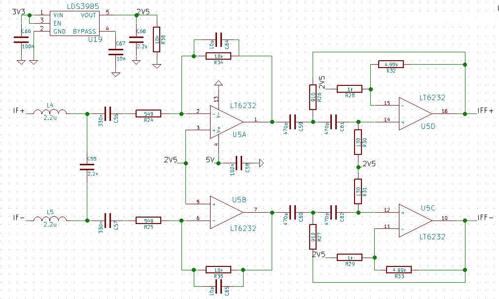
Baseband filter schematic. IF is output from mixer, IFF is input to ADC driver.
Received power by radar decreases as a fourth power of distance. This causes various problems, such as doubling the maximum detection distance requires 16 times more transmission power. Other problem occurs when there are several targets large distance apart. Target close to the radar reflects much more power than the farther target. Fourth power means when target is 10 timer farther, power received is ten thousand times smaller. Real hardware has limited dynamic range making it possible that close target with more powerful return signal masks the weak signal from farther target.
Because the frequency of the target in FMCW radar depends linearly from the distance to the target, it is possible to use high-pass filter to equalize the signals from far apart targets. If signal after the mixer is filtered using 40 dB/decade high-pass filter, responses from same sized targets from different distances will ideally have same amplitude.
In schematic above is a 40 db/decade high-pass filter implementing the range compensation. The first stage is LC-lowpass filter to filter out the high frequency noise before the first amplifier stage. After AC-coupling capacitors for removing the DC-offset is the first amplifier stage that amplifies the signal before more processing. Next stage is a 2nd order Sallen key high pass filter that generates the 40dB/decade slope. Output then goes to digital board which has a variable gain stage and ADC driver.
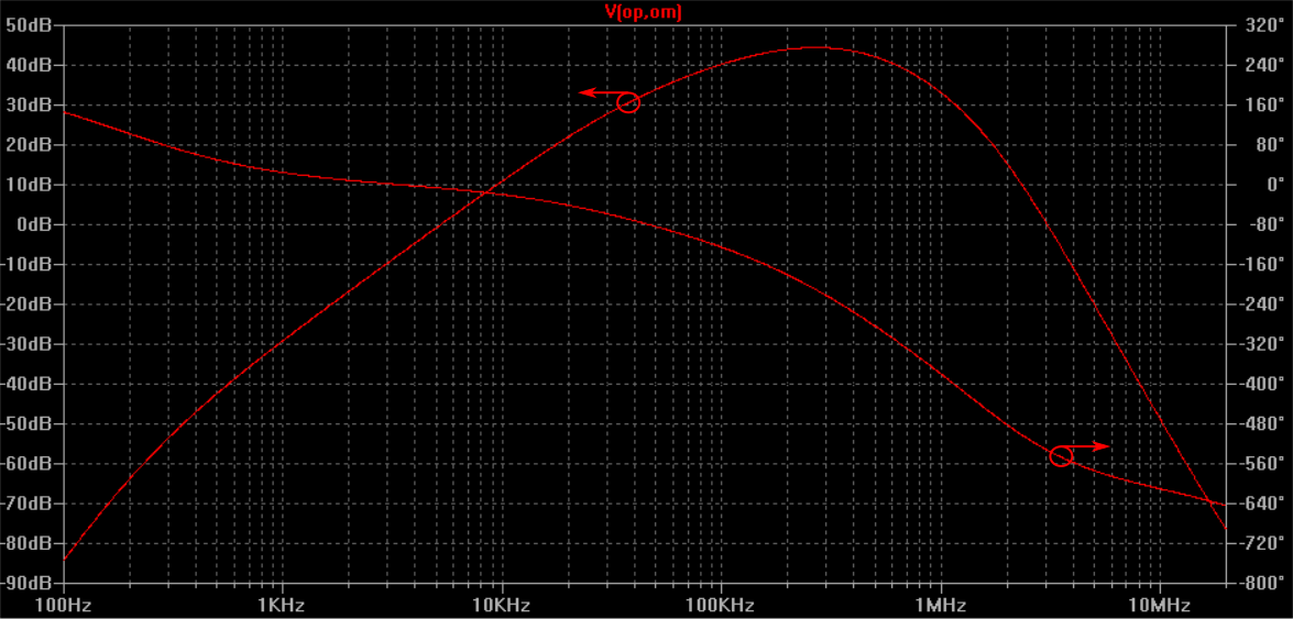
Baseband filter frequency response.
Downside of this approach is that at low frequencies baseband gain is much lower and it can even attenuate the signal. RF noise is still same at all frequencies, so low baseband gain reduces the dynamic range at low frequencies. In the end it doesn't really matter that much since at low frequencies dynamic range was already very high due to high received power.
Below is the same scene is simulated with and without the range compensation filter showing how big effect it can have.
Simulated received signal after mixer from several same sized targets at various distances.
FFT of received signal. Target very close to radar reflects so much more power that targets farther away are not seen. X-axis is frequency in Hz.
Same signal after range compensation filter.
FFT of filtered signal. Targets farther away are now also visible.
Soldering digital board
Backside has only few passives and is soldered by hand.
Backside is soldered first. It has only light components that stay in place by surface tension of the solder even while upside down during reflowing of the top side. Board-to-board connector is soldered after the top side is done, it is so tall that it would raise the board and make applying solder paste on the top side harder.
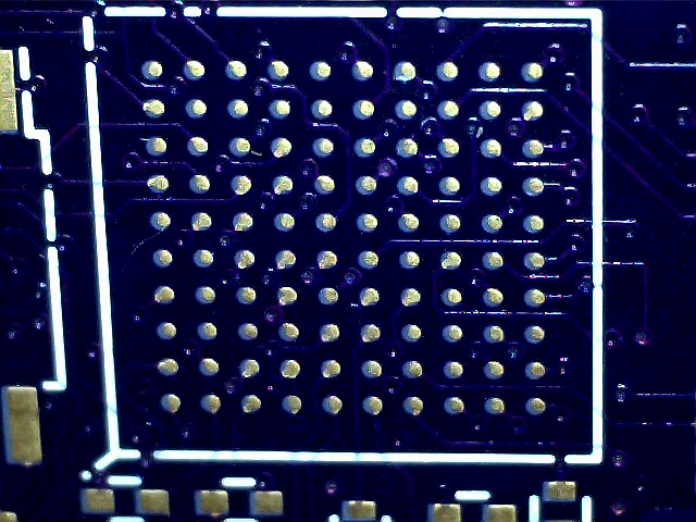
100 ball BGA footprint. Solder mask is applied slightly offset.
Spreading solder paste using stencil.
Close up of the BGA before reflow.
I managed to put the BGA pretty much perfectly on place, there's maybe about 0.1 mm of positioning error, but surface tension of the solder can correct it. Even bigger positioning error should be fine as long as balls don't bridge the solder paste drops.
Outline of the BGA on solder screen is very useful for positioning it. Without any visible guide on the board positioning would be very challenging as the pads are under the chip.
After reflow.
After reflow solder joints look good. It looks like the solder balls on the BGA also reflowed and combined with solder paste on the PCB. If only the solder paste reflow with balls staying solid everything might work for a while, but the contact between ball and small amount of reflowed solder paste isn't very reliable.
After reflow.
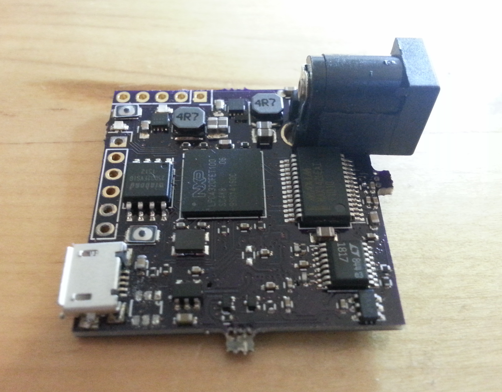
Chip on left is flash memory for firmware, center is microcontroller, right is ADC and below it is op-amp to drive it. Unpopulated component on the bottom left is USB power switch for USB on-the-go. I decided to leave it out since it can be switched from the microcontroller. If it is enabled while connected to computer it would short the on-board 5V to computers USB power line, which is why it's better to leave it out until everything else is working.
Two very small surface mount switches are reset button and USB bootloader button.
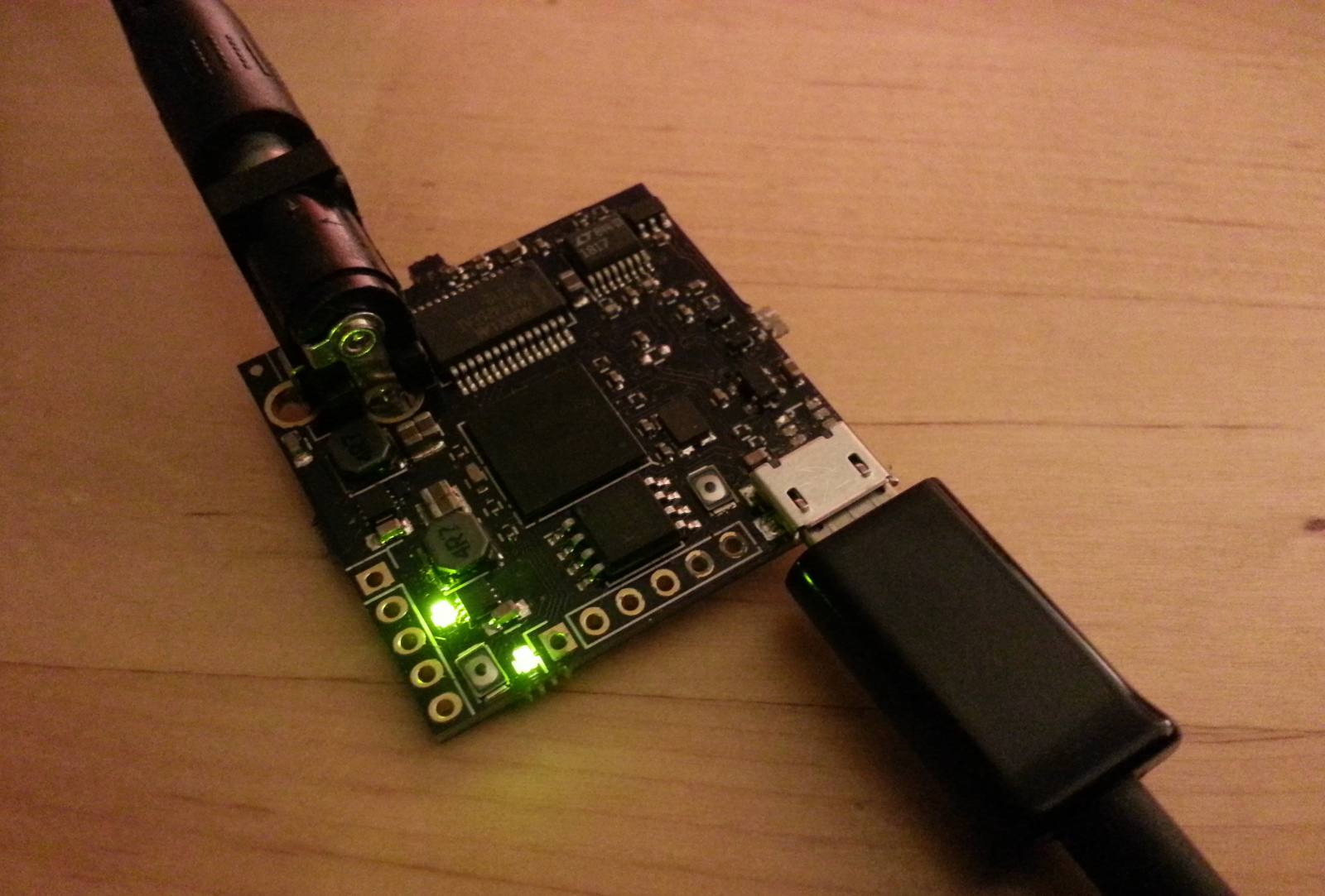
Microcontroller working. Other LED is controlled by the microcontroller.
Advantage of two board design is testing in parts. If there was a mistake in power supply circuit that would provide too much voltage, at least the other board would be saved.
Soldering RF board
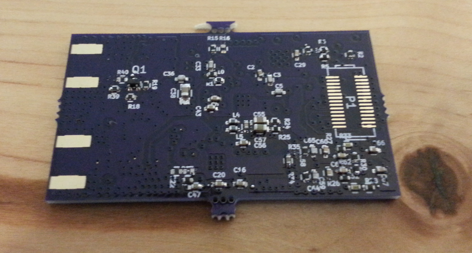
Backside of RF board.
To save money I didn't order stencil on bottom sides of the boards. There are only passive components with leads visible that are easy to solder without stencil. On top side are all the difficult to solder components which are much easier using stencil.
Paste on RF board. Missed a spot on top left corner.
Paste on RF board after removing the stencil.
Components soldered. Tabs on the sides are leftover from manufacturing of the PCBs, they could be snapped off but I haven't done it yet.
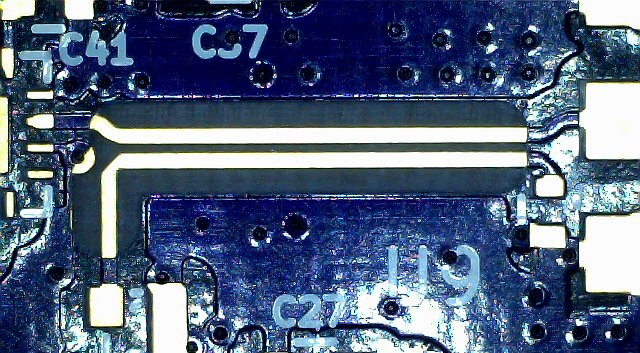
Shiny traces without solder mask are controlled impedance lines for high frequency signals. Solder mask would cause some additional loss and slightly change the impedance of the lines so it's better to remove it, though effect isn't very big.
Last time the traces were quite rough which probably had some effect on the matching. This time edges of the traces are etched very smoothly.
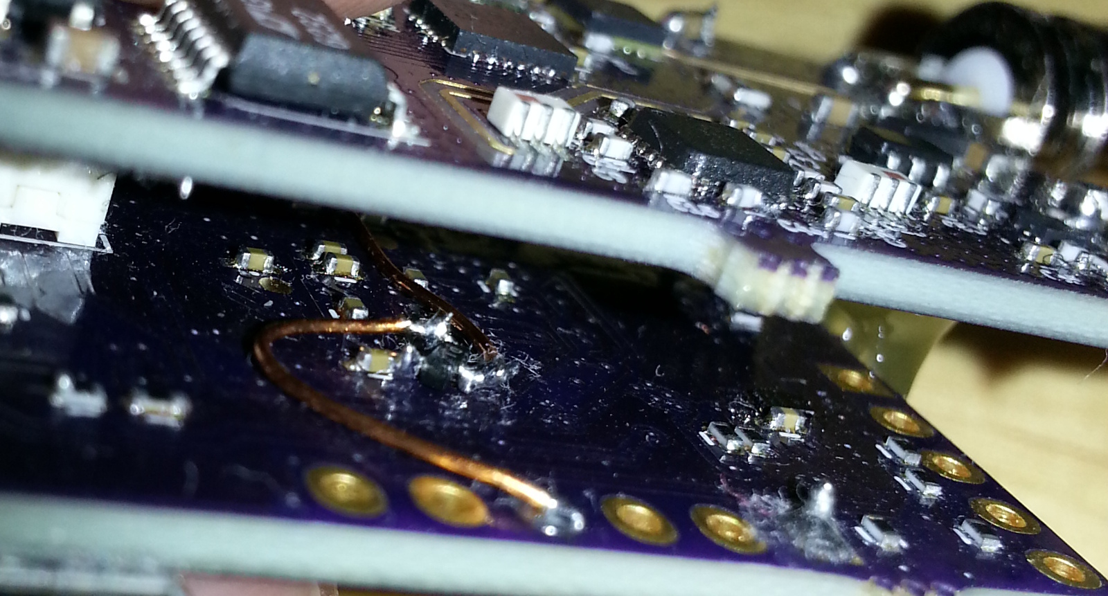
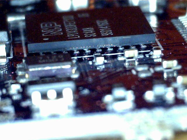
Jump wires and transistor.
Somehow everything ended up working without any bigger mistakes. One small mistake I made that required a jump wire was wiring the ramp complete pulse from PLL to general input of microcontroller. I was thinking I could put a pin-change interrupt on the pin, but this ended up not working. SGPIO buffers the samples from ADC so that it's not possible to know the exact sample that ramp was completed from interrupt. I had to connect also the ramp complete signal to SGPIO input and sample it for every sample from ADC.
This required adding a transistor to lengthen the pulse as input isn't anymore edge triggered. Pin is connected to the drain of the transistor with integrated pull-up resistor of the sourcing current and parasitic capacitance of the board slowing the signal. Luckily I had added a test pad to one of the unused SGPIO inputs, otherwise fixing it would have been impossible due to BGA package.
Also visible in the picture above is glob of hot glue holding the boards together. Mounting holes would have costed at least 10€ more in PCB costs so I decided to leave them out.
Range measurements
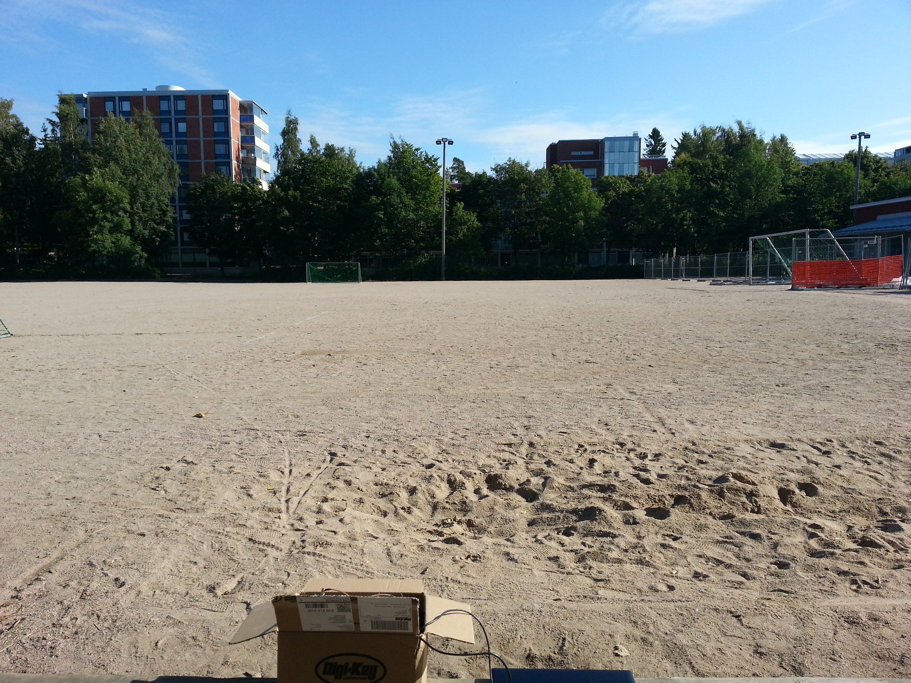
Image of the football field.
Easy way to measure radar range is to have radar pointing at empty area and then walk back and forth in its field of view. From the radar data it's then easy to see how the signal-to-noise ratio changes as distance to radar increases.
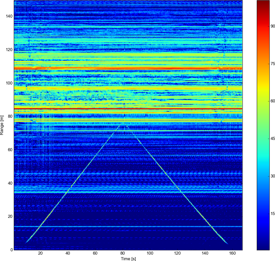
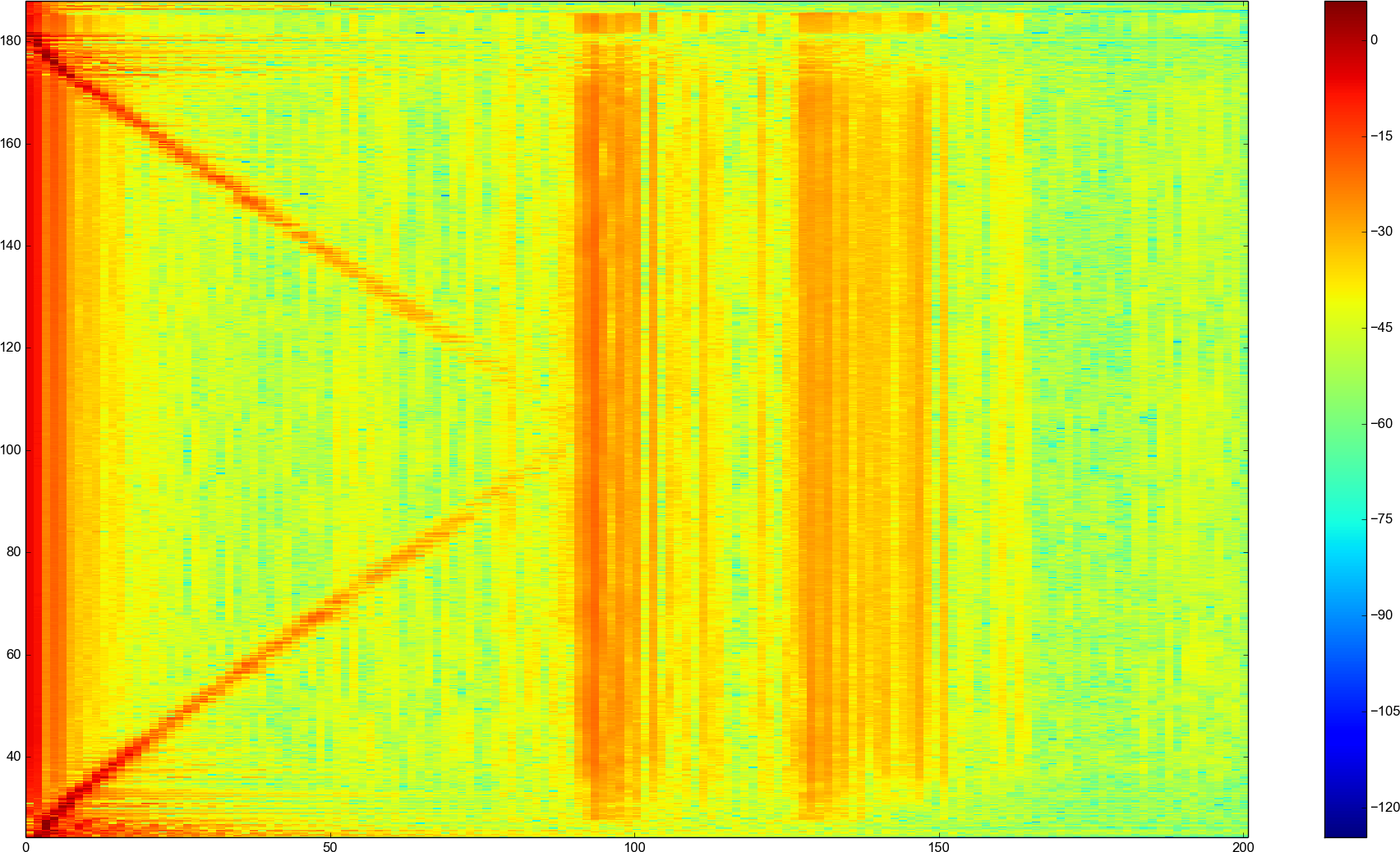
Time-range plot of me walking down a football field. Bandwidth was 700 MHz.
Above is a time-range plot of me walking back and forth a football field above. Lines around 35m are reflections from a football goal. Beyond 80m is a fence, some bushes and buildings which have large radar cross-section.
For antennas I used the same horn antennas I made for the previous radar.
Compared to same test from previous radar signal-to-noise and range resolution ratio are much better. Improved range resolution is caused by much larger bandwidth and more linear sweep. Increased bandwidth also increases signal-to-noise ratio as there is less clutter per range cell. More sensitive receiver has a big effect on the signal-to-noise ratio and because of range compensation both near and far targets are visible at the same time.
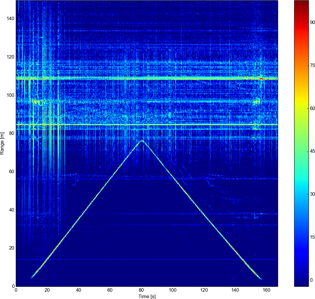
Reducting clutter by substracting the previous sweep from the next one.
Subtracting previous sweep from the current one in time domain should remove all the static targets since they should generate exactly same return. Small targets are removed, but some of the biggest are removed only partly.
When I'm close to the antenna, I'm shadowing the background which changes its reflection and doesn't cause completely perfect subtraction.
Wind can move the leaves a bit, even a millimeter of the movement will change phase of the signal and not cause complete subtraction. That's why my track is visible even though my movement between sweeps is only about one centimeter.
Clock drift between PLL reference and ADC sampling clock will also cause the subtraction to not be completely perfect. PLL reference and ADC clock are separate, but should have been derived from the same source for best accuracy. The small drift between them will cause phase of the baseband signal to vary a little and subtraction is not perfect.
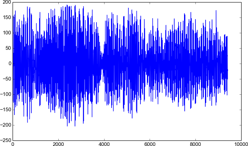
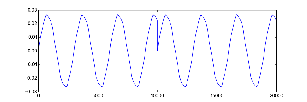
Time plot of the baseband signal. Y-axis is raw ADC values.
Above is the raw baseband signal from ADC. Due to high pass filter high frequency returns from far away targets and low frequency returns from near have about same amplitude.
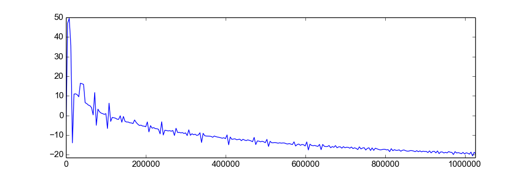
Fourier transform to get distance.
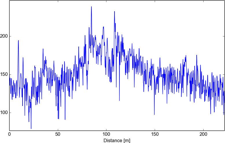
Taking Fourier transform of the ADC output gives the distances. This is from the beginning and reflection around 9 m is from me. Signal-to-noise ratio is about 60 dB.
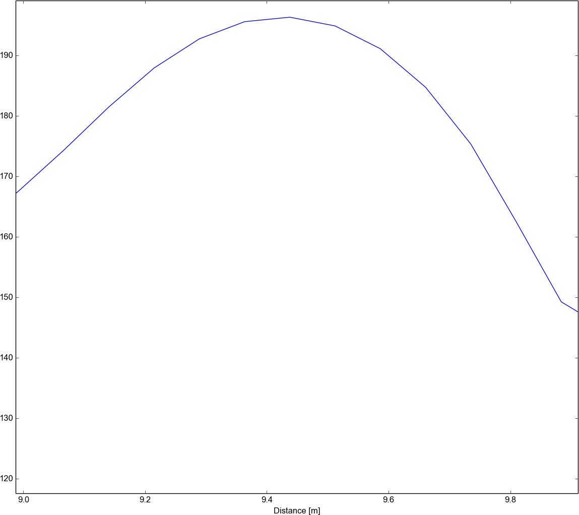
Zoom around 9 m.
Resolution of radar depends on its bandwidth with higher bandwidth giving better resolution. It should be noted that resolution only means being able to detect nearby targets as separate. Accuracy of the distance depends only on accuracy of clocks of the radar. Padding signal with zeroes smooths the FFT and allows to locate the peak with much better accuracy. Zooming into the 9 m peak reveals that my position at that moment was about 9.43 m. Unfortunately I don't have means to verify this to required precision.
Synthetic Aperture Radar
Besides measuring the distances, radar can also be used to generate two-dimensional images of the scene. This can be done by measuring several distance profiles while radar is moved on a straight line with antenna looking sideways from the direction of travel. If the antenna radiation pattern is very narrow, range profiles can be stacked to make image of the scene. Issue with this method is that assumption about the narrow beam width can't often be fulfilled. Antennas I'm using have beam width of about 40 degrees and resolution in direction that radar was moved (cross-range or azimuth) would be horrible.
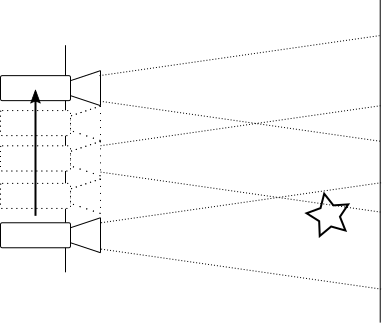
SAR system diagram. As radar moves along the line targets inside the antenna radiation pattern change.
Synthetic aperture radar is a signal processing method of achieving much better cross-range resolution from same range profile measurements. It uses many range profile measurements along a line to synthesize antenna that is as long as the line radar moved in. Beam width of an antenna is related to its physical size and very long synthesized antenna has very small beam width giving much greater cross-range resolution.
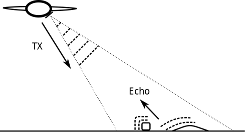
Airborne SAR system diagram.
Typically SAR imaging systems are mounted on either airplane or satellite so that it can look at large area of ground from angle. Radar sends pulses to ground which reflects them back and gives information about distance to the scene being imaged.
To get reflections from the ground and avoid shadowing from big structures antenna of the radar needs to be mounted in angle. If angle is too big and antenna points straight to ground range resolution is poor since all of the reflections come from almost same distance away. If angle is low and antenna points along the ground then tall structures such as buildings and hills can hide other objects behind them and flat objects like ground don't reflect signal back to the radar since reflection angle is too shallow.
Unfortunately I don't have a spare airplane so I mounted the antenna on bicycle pointing in zero angle. This means that only tall vertical structures like lamp posts, building walls and trees reflect the signal and image looks like cross-section of the imaged area.
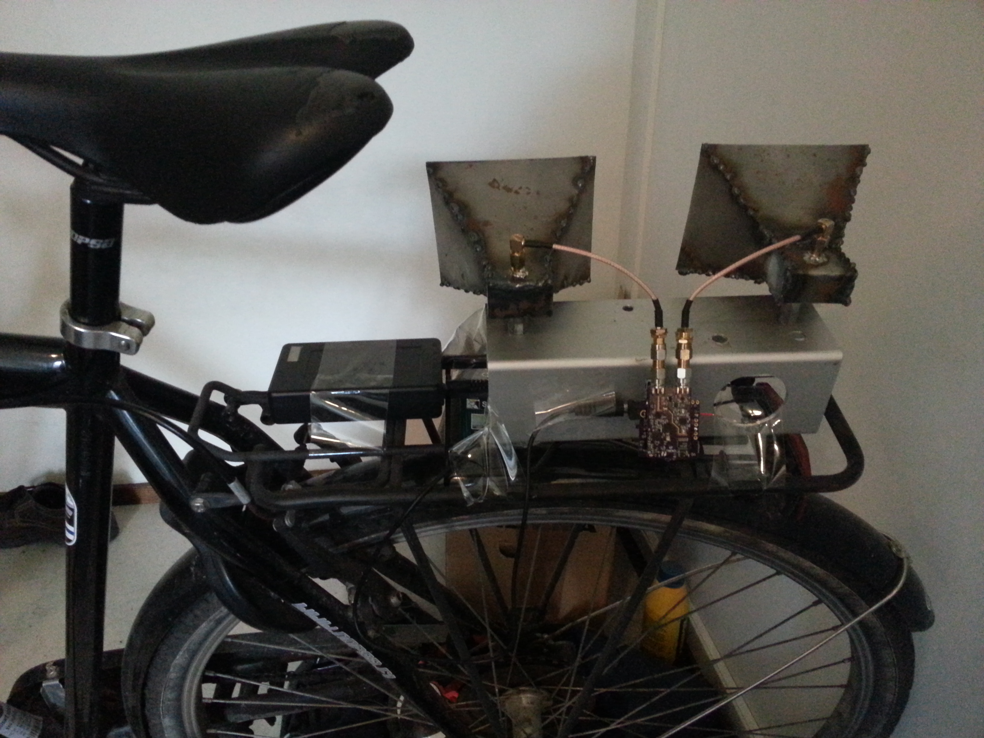
Radar mounted on bicycle for SAR imaging. Antennas have started to rust a little.
To properly focus the SAR image, platform (bicycle) needs to move at constant speed in straight line, this is relatively easy to do even on bicycle if ground is flat. Antenna should also point in the same direction. Tilting the bicycle will cause it to point to ground or sky and change the radar return. Tilt of few degrees shouldn't affect the image too much because of large antenna beam width.
Hard part is that path needs to be very straight because phase of the return signal is used for focusing the image. Phase of the baseband radar signal wraps around when radar moves half wavelengths of the carrier frequency. In this case carrier frequency is about 5.5 GHz making the wavelength 5.5 cm. To be properly focused error in path linearity should be around less than tenth of a wavelength, which is only 5 mm. It is very challenging to move in this straight line for several meters and some amount of defocusing from movement is expected.
Cross-range size of the image depends on the length that platform traveled, but going larger distance also means that motion errors are larger which increases defocusing of the image. Proper SAR imaging systems use GPS and very accurate and expensive inertial measurement units to measure the actual motion of the platform and take it into account when focusing the image. Phone GPS doesn't have high enough resolution and I don't have inertial measurement unit so I just needed to try my best to keep constant speed and straight path.
I decided to try taking a SAR image of the nearby football field where I tested the radar before. Right next to it is paved road that is very flat minimizing the motion errors.


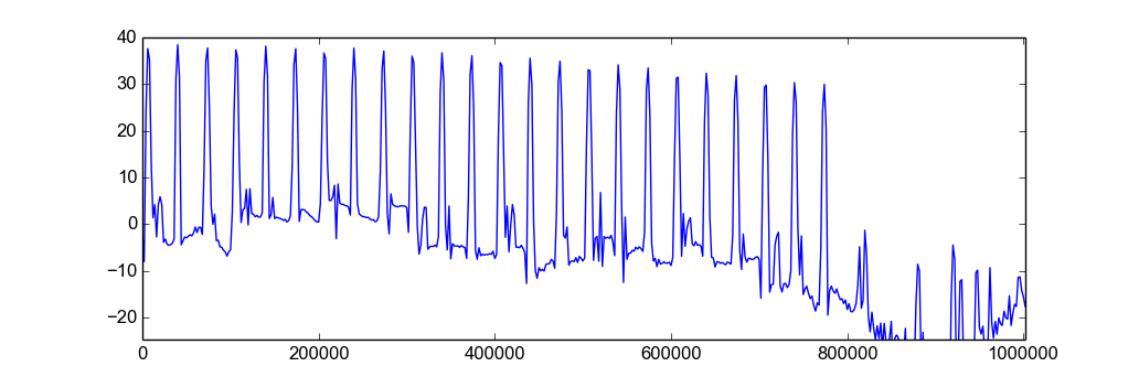
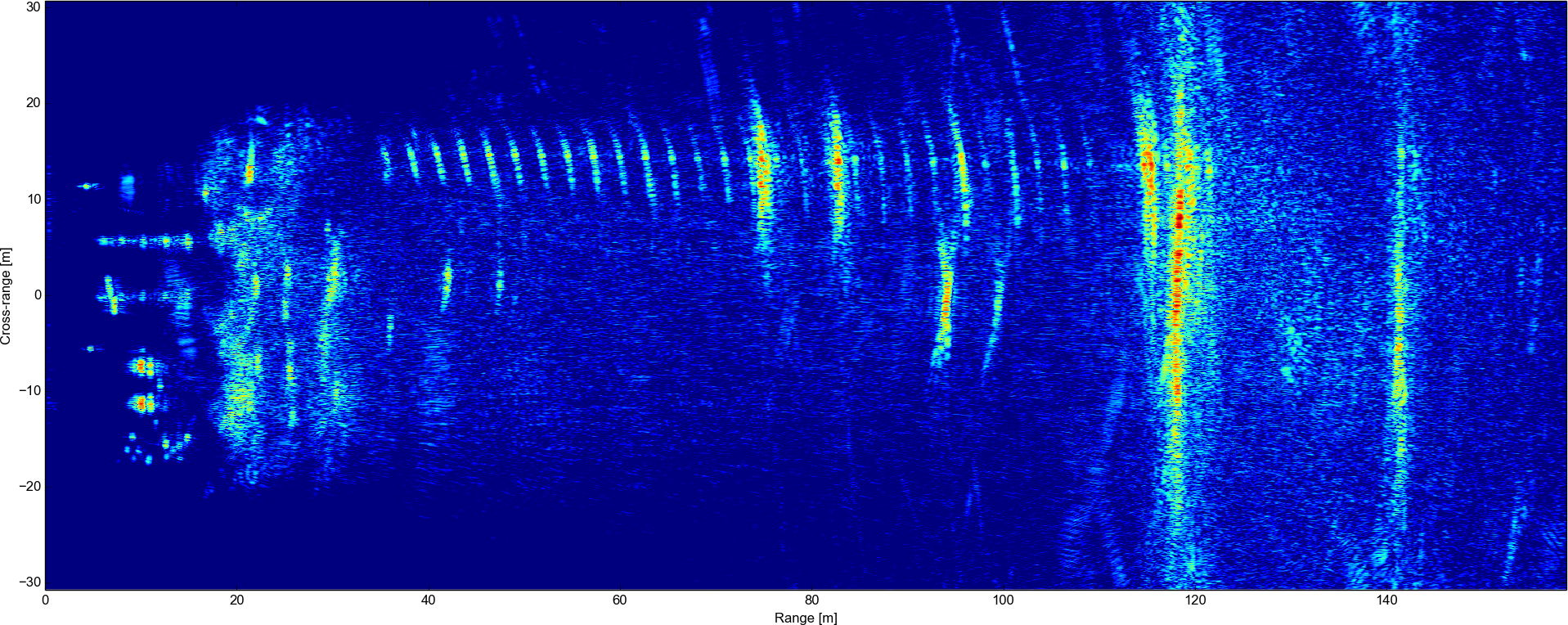
Above is the raw range data from radar before SAR focusing. As expected the method of just stacking range profile doesn't result in very high resolution image. Format is the same as in stationary range-time plots before but now the radar is moving. Y-axis is range in meters and X-axis is samples. Sweep time was 2 ms, track was about 30 m long and bicycle speed was approximately 1.4 m/s. This works out to one sweep every 2.8 mm and for signal processing it can be assumed that radar was still while sweeping. This is called stop-and-go approximation and it simplifies the signal processing. Only every tenth sweep was used for image focusing.
SAR focusing algorithms are a big topic that you could write a book about. In short there are several algorithms for focusing SAR images designed for different imaging geometries. The one I'm using is omega-k algorithm, which is also called range migration algorithm.
When radar moves along the line targets on the radiation pattern of the antenna stay visible for some distance on the line. Because radar measures direct distance to the target, returns from the target shows as arcs due to changing distance to it. These arcs are very clearly visible in the raw data image above spanning wide area of the image due to wide antenna radiation pattern. Before cross-range focusing can be done this range migration must be corrected.
Omega-k algorithm corrects the range migration using process called Stolt interpolation on the Fourier transformed raw data. As a result energy from same target is lined on a same range cell and inverse Fourier transform can be used to focus the image. More detailed explanation and mathematical derivation can be found in example from this thesis[PDF]
Above is the resulting focused SAR image of the same raw data above. Resolution is greatly increased and now some of the features of the scene can be seen. Still lack of focus can be seen especially on the fence posts in the middle of image. Each post is smeared in cross-range direction several meters due to motion errors during the imaging.
Camera picture above is taken at +8m cross range. Bigger fence post of green metallic fence on the left in the camera image have high radar cross-section and are very clearly visible in the SAR image. Bicycle racks are visible as lines. Radar signal passes relatively easily through the trees on the foreground, but metal fence at the end of the field at 120m reflects very strongly. Still some of the signal goes through it and reflects from building across the street.
To focus the image better, I wrote a minimum entropy autofocusing[PDF] program. When image is in focus it is sharper and its entropy is lower. Minimum entropy autofocusing algorithm picks a phase shift for each sweep that minimizes the image entropy.

Autofocused image is much sharper. Now the fence posts have much better resolution, but there are still some places in the image that are not perfectly focused.
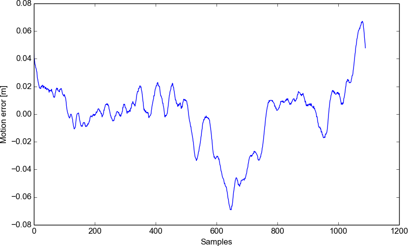
Motion error from autofocus.
Calculated motion error is few centimeters. Most of the remaining lack of focus is probably caused by non-constant speed of the bicycle as autofocusing algorithm can only correct motion error in range-direction.
Note that autofocusing algorithm didn't enforce any continuity or other structure on the phase error. Still the solved phase error is very physically reasonable. Antenna couldn't have moved too much during the few milliseconds between the sweeps and phase error difference between adjacent sweeps is small as expected. I find it surprising that using optimization goal as simple as entropy of the image works this well.
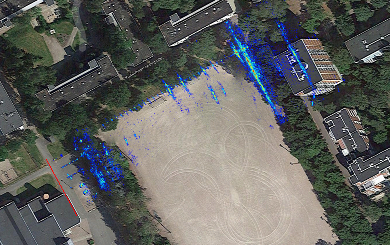
When overlaid to image of the field from Google maps, SAR image agrees well with it. Football goals have moved a little since map has been updated, but everything else is where it should be.
Conclusion
Total cost was about 200€. PCBs were 28€, components were about 120€, battery pack was 21€ from China and antennas were made from scrap metal.
All hardware design files, firmware and processing software is available at github.