All of the best integrated circuits today come in hard to solder BGA packages. Because BGA packages have connections under the chip soldering is harder and it needs to be done using a reflow oven or hot plate. Another problem is with designing the PCB, vias and traces need to be small enough to fit between the solder balls and there needs to be usually quite many layers in the board to make room for all the closely packed traces. This means that a cheap Chinese two layer board doesn't have enough room and more layers are needed. Adding layers increases the cost of the board dramatically when ordering only a few copies.
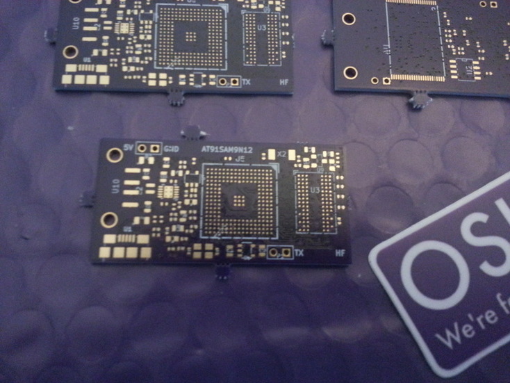
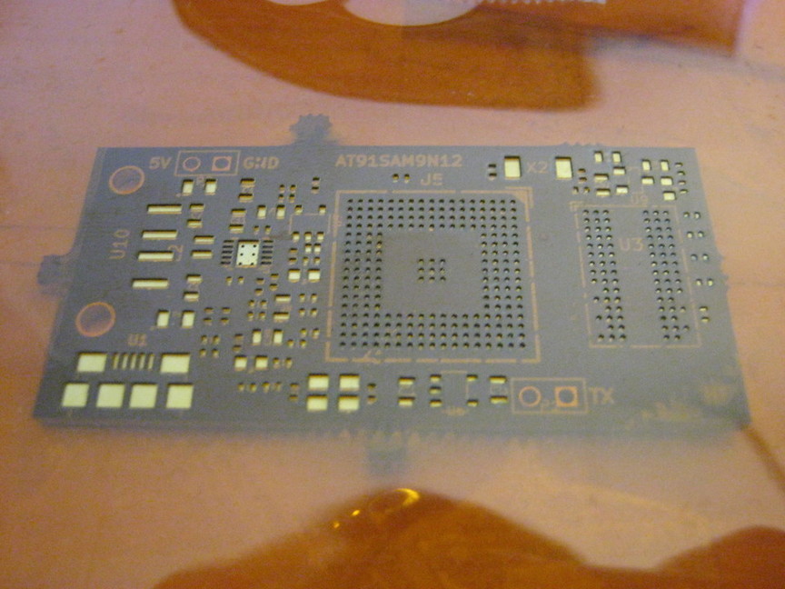
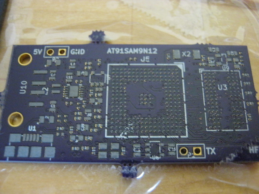
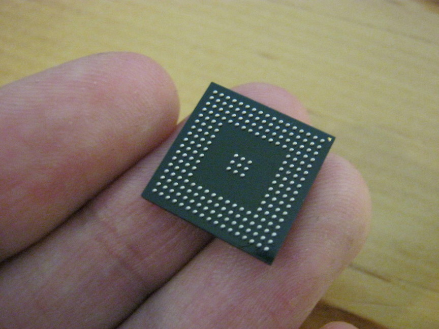
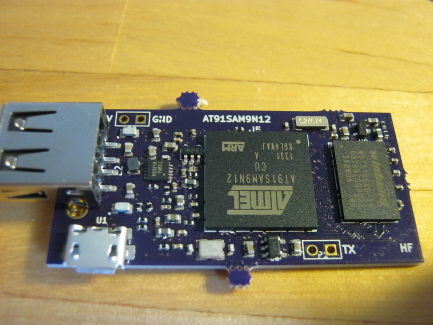
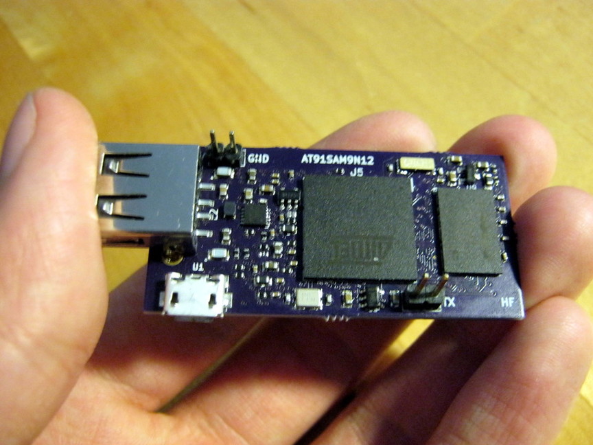
I wanted to try designing a board with BGA chips in it to see how hard soldering them could be. So I decided to design a small ARM embedded system that can run Linux. ARM processor that I decided to use was AT91SAM9N12 in a 217 ball LFBGA package, just because it was the cheapest ARM processor with memory management unit which is required to run Linux. Originally I wanted to have only one BGA chip, but RAM in BGA package was significantly cheaper than in other packages and I decided to also have DDR2 memory in a BGA package.
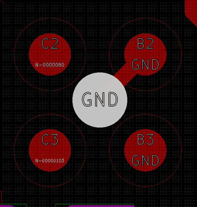
Positioning VIA for maximum amount of space.
Finding a manufacturer for the board turned out to be a slightly challenging task. Two layers wouldn't be enough and at least four layers would be needed. Ball diameter of the 217-LFBGA package is 0.4 mm and distance between adjacent balls is 0.8 mm. To make a little bit more room for the vias ball land pattern can be made slightly smaller than the solder ball. I used 0.36 mm pads. Putting via between the four balls maximises the available space. Manufacturer needs to be able to make a via that fits in about 0.8 mm space. Almost any manufacturer can make a via with this diameter, but the problem is that this distance includes via drill diameter, two times the annular ring around the via and two times the minimum distance between via and trace. For example iTead's four layer board has minimum via drill diameter of 0.3 mm, minimum annular ring width of 0.15 mm and minimum 0.15 mm between via and trace. This adds up to 0.9 mm which means that minimum sized via can't fit between the BGA balls. The only reasonably priced manufacturer I found was OSH parks. Their four layer board has smaller limits and via can just barely fit between the BGA balls. As a bonus it's also cheaper than iTead for small board.
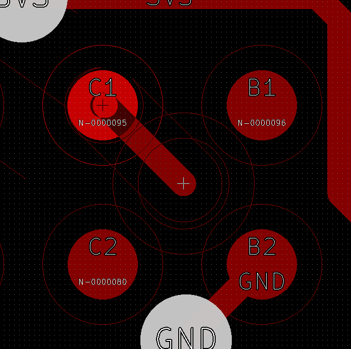
Minimum via with OSH park design rules, fits just barely
Even though the via can fit between the BGA balls, there are still some problems: There is not enough room for trace to go between two vias. This means that it's not possible to route the BGA using standard escape routing where every pad has one via. This means that board needs to have enough unconnected pads on the perimeter, so that traces from the inside can be routed. Fortunately the processor has many general I/O- pins that are left unconnected.
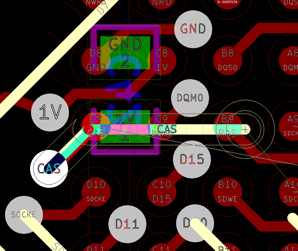
... but trace doesn't fit between two vias without violating the design rules. CAS trace doesn't have enough room to fit between DQM0 and D15 vias.
Manufacturing concerns solved, it's time to start thinking what components should be on the board. I don't really care about the usefulness of the board and this whole project is more of a learning experience. To keep the costs down board size needs to be kept small. This means that there won't be space for any extra interfaces like ethernet, serial ports or SD-card.
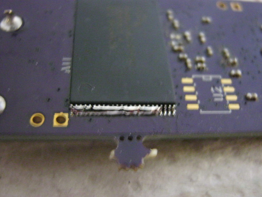
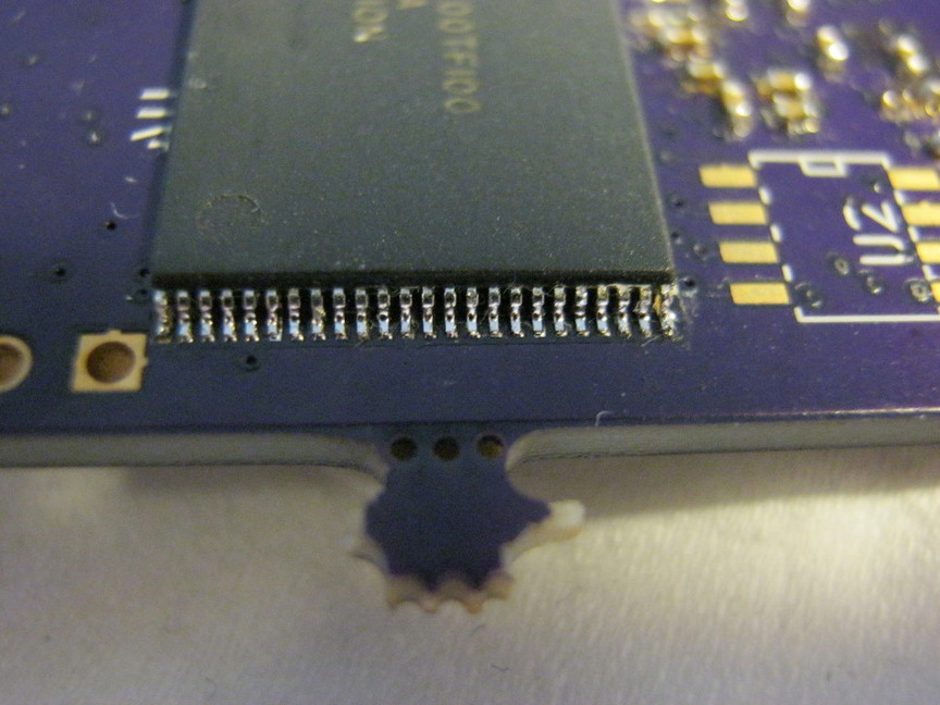
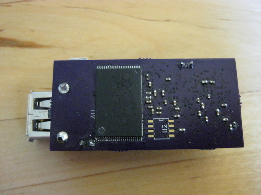
Besides the processor and RAM other essential components are: mass memory, voltage regulators and supervisor circuit for handling the reset of the chip. Processor can boot from the NAND, but I decided to also have Dataflash for the bootloader just in case, though this ended up being left unpopulated. For mass memory NAND flash is a good choice because it's cheap with big capacity. Having it also in a BGA package would have been cheaper, but I already have enough trouble with two BGA packages, so I decided to use 4Gb NAND in a 48 pin TSOP package.
Connecting the components is explained well in the processor's datasheet, but because the document is over 1000 pages long it might be hard to find all the details. Atmel also publishes schematics of the evaluation boards that are very helpful when designing a board.
Some freedom needs to be taken with DDR2 traces. Normally traces should be length matched, have controlled impedance and terminating or series resistors. Reference design from the development board uses series resistors in all of the DDR2's signals. I don't have enough room for them so I just decided to leave them out. Impedance isn't 50 ohms either, because I had to use smaller traces to fit everything. I hoped that because RAM is so close to the processor, lack of series resistors and impedance mismatch wouldn't matter. All traces from CPU to RAM are about 25 mm long. Usual rule of thumb is that if trace length is over 10 % of wavelength of the signal then transmission line effects should be taken into account. In this case it would mean that frequency should be roughly above 1 GHz. RAM clock frequency is only 133 MHz and even the first few harmonics are under the 1 GHz, which suggests that this should work fine. Just to be sure I matched the trace lengths within few millimeters, but this might have been unnecessary.
Voltage supplies are bit complicated. Processors core voltage is 1.0 V, RAM needs 1.8 V and NAND needs 3.3 V. Because the input voltage is 5 V from USB, board needs to have three different voltage regulators. Normally it would be good to reserve one layer on the board for power supplies and keep it free from signal traces to lower power supply impedance, but board only has four layers and one of them is used for ground plane. This would mean that there would be only two layers left for signals which wasn't enough. So I didn't have separate power supply layer and instead made several planes in different layers for different power supplies.
Losses with linear regulators would have been too big for USB powered applications in the worst case, so I decided to have 3.3 V regulator as a more efficient switching regulator. 1.0 V and 1.8 V regulators are linear regulators that have 3.3 V as input voltage. Because linear regulators losses depend on the difference between input and output voltage using 3.3 V as input instead of 5 V increases the efficiency.

Schematic. Click for a pdf version.

Soldering
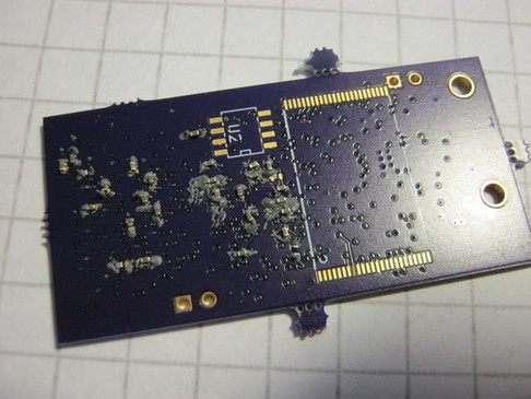
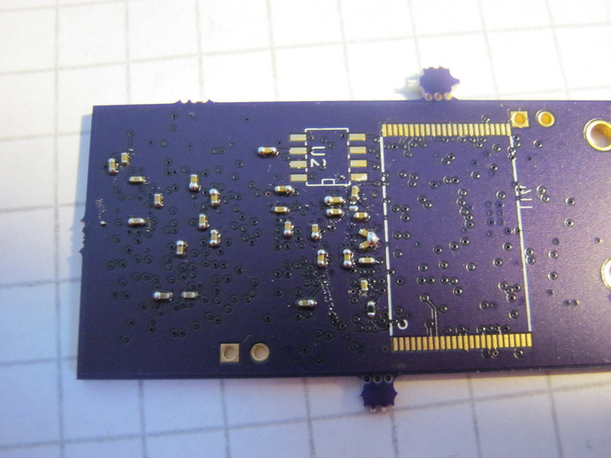
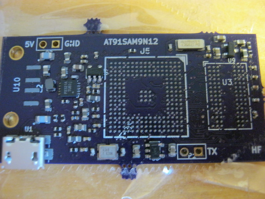
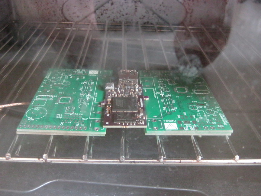

After plugging the USB cable to the USB device port nothing has exploded and I can see that a new serial port /dev/ttyACM0 has appeared and opening it with SAM-BA program, which is used to program the bootloader and kernel, everything seems to be working. Many people say that soldering BGAs is hard but based on this experience I can't agree. Maybe I just got lucky but I didn't have any problems with them.
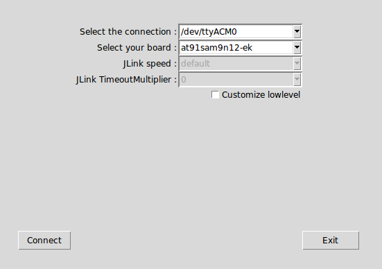
Opening SAM-BA. At91sam9n12ek is Atmel's development kit for this processor and its configuration also works for this board.
Software
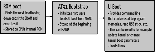
Boot flow graph
Bootloader
Boot process start with internal ROM bootloader trying to find a valid program in different memories. It probes SPI flash, SD card, NAND flash, second SPI flash and I2C EEPROM for a valid program. If it finds one it starts it, otherwise it enters into SAM-BA monitor, which is debugging mode where processor listens serial and USB port for commands. This mode allows programming the bootloader.
ROM boot can't boot Linux kernel directly so a second stage bootloader is needed. It will initialize RAM and clocks and then load the Linux kernel. AT91 Bootstrap is a ready made bootloader that does all of this. It will be stored at the beginning of the NAND flash it could also be placed to Dataflash if I had populated its footprint. Even though AT91 bootstrap could boot Linux directly it's more useful for debugging to have U-boot bootloader after it. U-boot is its own mini operating system with command line and it can read USB sticks, use ethernet, write and read from NAND and of course boot Linux. Using U-boot makes it easier for example to erase NAND or change Linux boot parameters.
To compile the bootloader an ARM cross compiler is needed. I'm using Sourcery codebench lite edition, because it's very easy to set up and works well. It's easiest to first load AT91SAM9N12EK development board configuration file. Modifying this configuration file saves a lot of trouble compared to writing new configuration file from scratch.
To make it work for this custom board some changed are needed: RAM size needs to be configured to 64MB, number of banks changed to 4 and some latencies tweaked (Evaluation board has 128MB of RAM with 8 banks). NAND initialization function also needs to be modified, this board has NAND flash connected to different place than the development board and it's necessary to tell the bootloader about it.
U-boot
Configuring U-boot is very straightforward now that AT91 bootstrap has initialized the hardware. It also has configuration file for at91sam9n12ek, but it's set up to boot from SD-card by default. There aren't many other required changes to make, because hardware is already configured. Some optional ones are enabling UBIFS tools for creating and editing partitions on NAND flash and enabling support for reading ext4 formatted USB sticks. USB support makes it possible to boot Linux kernel from USB stick, which makes easy to experiment with different kernel configurations.
Linux and root filesystem
Installing Linux isn't as easy as with a regular x86 PC. Kernel needs to be configured to support all required devices and the root filesystem image needs to be built. This could be done by hand, but it's easier to use buildroot which is a set of makefiles for building the root filesystem and kernel. Still the process can be a little hard because of massive number of different options in kernel and buildroot.
Buildroot doesn't have configuration file for at91sam9n12ek development board, but it has a file for other Atmel board, at91sam9260ek. Using this configuration as a base will makes the configuration little easier. These settings can be loaded with "make at91sam9260ek_defconfig".
First we want to have a relatively new kernel version, because there have been some minor changes related to this processor. So let's use version 3.15.3, which was released last week.
Linux is configured in buildroot with "make linux-menuconfig" command. It will open the usual Linux menu configuration window. Most important configuration in the kernel is system type configuration menu. We need to check AT91SAM9N12 support and "Atmel AT91SAM Evaluation Kits with device-tree support" option. Device-tree is an external binary file that is loaded with the kernel which describes the hardware available on the board. This makes it possible to use same kernel with different boards and device configuration for different boards can be made using text files instead of writing slightly different C-files for every board. Luckily there exists a device tree file for at91sam9n12ek which can be used as a base. Required changes are basically removing the devices that are not available. Path to this modified device tree file needs to be added to buildroot configuration so that it knows to compile and build an image out of it.
Other options worth enabling in the kernel are:
- USB host support AT91_USB.
- NAND flash support and processor's internal NAND ECC controller (PMECC) support.
- Support for UBIFS, which is going to be used as a root filesystem.
- Ext4 support for reading USB stick.
In buildroot configuration we need to choose what programs we want to have on root filesystem and the options for generating the root filesystem image. This board has raw NAND memory without controller so usual desktop filesystems such as ext4 can't be used. UBIFS is the usual choice and it's also fine in this case.
UBIFS has several options that depend on the NAND flash type and if they are wrong Linux can't read the resulting filesystem. These options could be figured out from the NAND flash datasheet, but easier way is to boot Linux from USB stick and create ubi partition from there. Or alternatively use U-boot's "ubi info" command which will read the NAND and output the required configuration values.
After typing "make". Buildroot will download cross compiler, Linux kernel and all of the other packages; build them and output kernel, device tree and root filesystem images. These can be transferred to board with SAM-BA program. Same program is needed to program NAND ECC controller parameters. Same parameters should be also configured to AT91 bootstrap, U-boot and Linux kernel or otherwise they will report that NAND is corrupted. In this case NAND has 2048 byte pages with 512 byte sectors and ECC should be able to correct 4 bits per sector. NAND addresses to store all the images can be found in AT91 bootstrap and U-boot configuration files.
After programming the board and resetting, the ROM bootloader should find the AT91 bootstrap on the NAND and start the boot process:
If you are interested in learning more, hardware and software files are available at github.
UPDATE 2014-08-10:
I ran memory test on the RAM and there were some errors. Rarely, about once per loop on memtest, there was an error on 19th bit on random write test.
1 2 3 4 5 6 7 8 9 10 11 12 13 14 15 16 17 18 19 20 21 22 23 24 25 26 27 28 29 30 31 32 33 34 35 36 37 38 39 40 41 42 43 44 45 46 47 48 49 50 51 52 53 54 55 56 57 58 59 60 61 62 63 64 65 66 67 68 | |
This probably means that the error is with D3 trace. It's the longest data trace and runs parallel to some address lines for short runs. Hard to say for sure what the cause is, but it is related to signal integrity as this chip should be able to run at 133MHz reliably. Despite the errors, this configuration worked well enough that no kernel panics or anything related to bad memory was observed during the normal operation. Issues seems to arise only when memory is stressed.
If clock speed is decreased to 100MHz memory seems to work fine. I have run memtester for over 10 hours consecutively and no errors have been found.