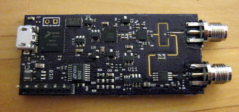
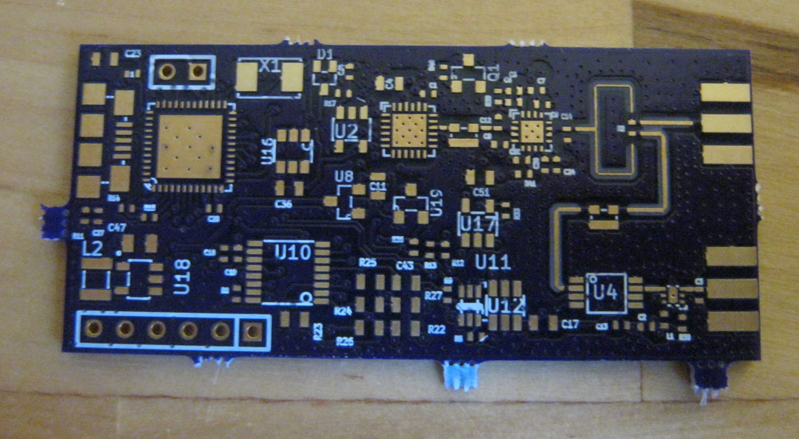
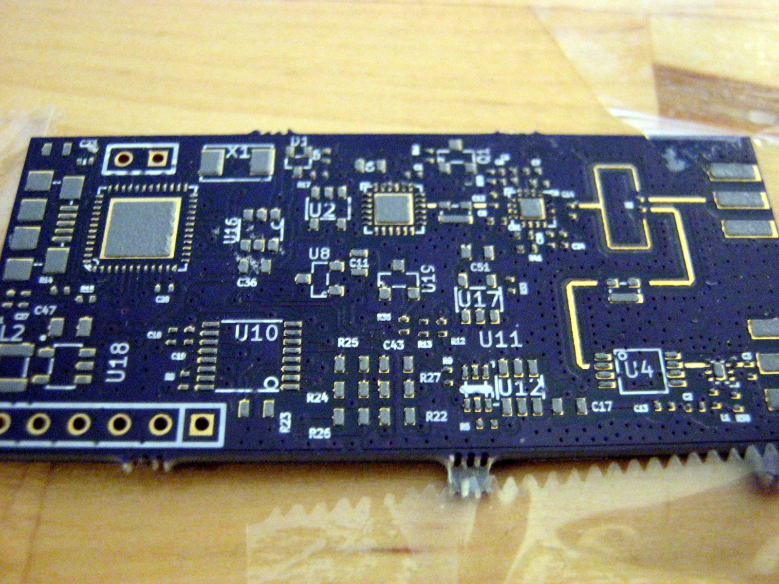
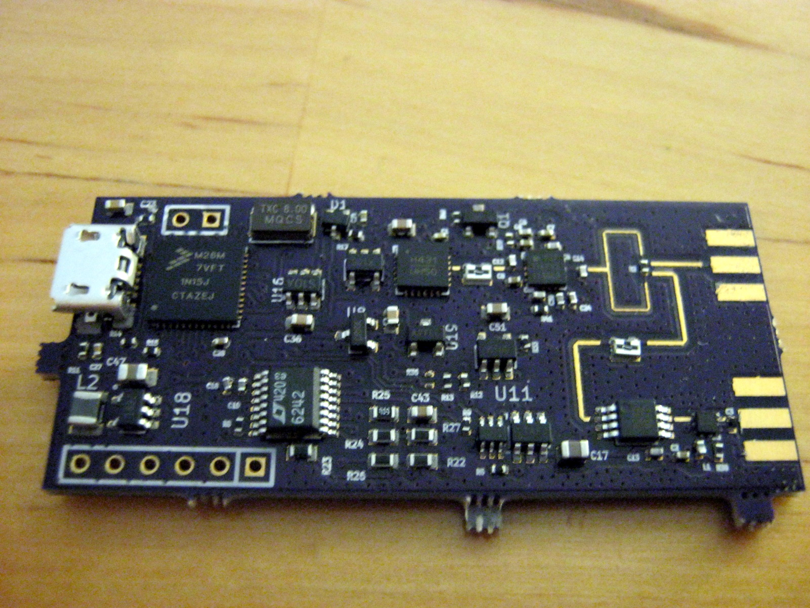
Finished radar board without antennas.
Introduction
I've for some time now wanted to do more RF design. Although I have taken some RF design courses, I haven't actually made a single RF design before. But you can't learn without doing and inspired by the MIT coffee can radar designed by Gregory Charvat, I figured that building a radar should be a doable project that would offer some challenge while also having some real world use.
The simplest radar is a continuous wave Doppler radar, which continuously transmit a constant frequency signal. This signal reflects from a moving target and Doppler shift causes reflected signal to change frequency. This reflected signal is then received and mixed with the transmitted signal. Mixer product is the difference of the frequencies which is proportional to the speed of the target. This kind of radar is very simple to make, in fact there are even some children's toys. Unfortunately it can't detect the range of the target and isn't that exiting.
A little more sophisticated radar which can detect also the range can be made by modulating the frequency of the transmitted signal. This kind of radar is called continuous wave frequency modulated radar (FMCW radar).
Radar transmits a chirp, which increases linearly with the frequency. This chirp is then radiated with the antenna, it reflects from the target and is received by the receiving antenna. On the reception side received and undelayed copy transmitted chirps go to the mixer. Because received chirp reflected from the target, but copy of the transmitted chirp is undelayed there is delay between the signals. This causes mixer output to have a low frequency signal which frequency depends on the distance to the target. When there are several targets the output signal is sum of different frequencies and the distances to the targets can be recovered with Fourier transform.
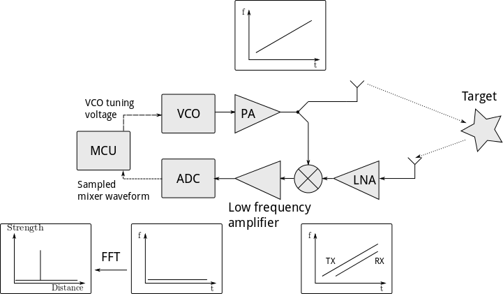
FMCW radar block diagram
Glossary of the terms in the block diagram:
- MCU - Microcontroller
- VCO - Voltage controller oscillator
- PA - Power amplifier
- LNA - Low noise amplifier
- ADC - Analog to digital converter
- FFT - Fast Fourier transform
Transmitted signal is: \(f(t) = sin\left( 2\pi\left(\frac{f_0 + f_1}{t_{\text{ramp}}}t+f_0\right)t\right)\) and the received signal is a delayed copy of it, \(f(t-t_d)\). Mixer multiplies these signals, outputting two frequencies which are the sum and difference of the multiplied signals. These can be solved using the trigonometric identity: \(\sin\phi \sin \theta = \frac{1}{2}\left(\cos(\phi-\theta)-\cos(\phi+\theta)\right)\). Sum frequency is too high to be detected and is filtered out. Frequency of the difference term gives: \(f_{\text{diff}} = \frac{t_d (f_1-f_0)}{t_{\text{ramp}}}\). Since electromagnetic waves travel at the speed of light delay of the received signal is twice the distance to the target divided by the speed of light. Distance to the target in terms of the detector frequency can be solved to be: \(d = \frac{c f_{\text{diff}} t_{\text{ramp}}}{2(f_1-f_0)}\).
For example with \(f_0\) = 6 GHz, \(f_1\) = 6.1 GHz, \(t_{\text{ramp}}\) = 5 ms, \(d\) = 100 m the output detector output frequency is 13.3 kHz, which is low enough to be detected with very cheap equipment. Even a PC soundcard would have enough bandwidth and this is actually how the MIT coffee can radar works.
How about the Doppler shift? It can be found out in two ways. If the frequency waveform is sawtooth wave, then we can take multiple consecutive range measurements and then take another FFT over them. Because movement of the target also changes the distance to it speed can be recovered and distance corrected.
Another way is to modulate the frequency with triangle wave. Doppler shift causes the mixer output frequency to be different depending on whether the frequency is increasing or decreasing.

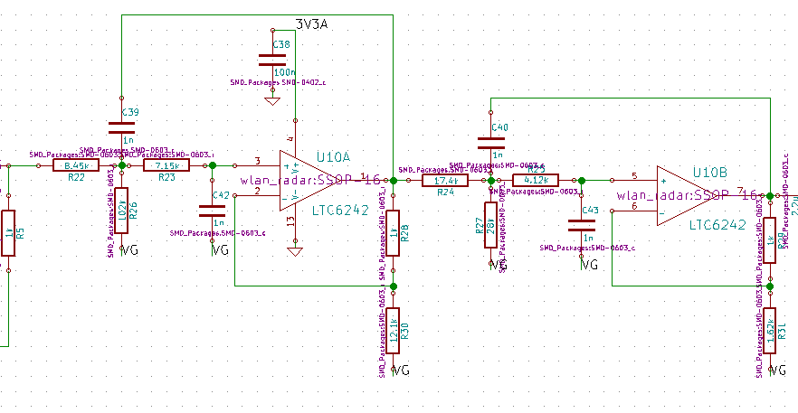
Schematic. Click for a pdf version.
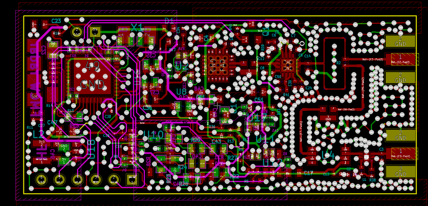
Board layout in Kicad without zonefills
Designing the radar
For radar applications high frequency is needed for smaller resolution. High frequency also allows using smaller antennas because wavelength is smaller. Unfortunately going to too high frequencies is going to get too expensive, component selection starts to be very limited and the RF design starts to also get much more difficult. 2.4 GHz would be very easy and cheap to design for because there are many different and cheap components for this frequency range due to it being used for many different purposes such as WLAN, microwave ovens, radios and more. Another frequency range where there also exists some more use and cheaper components is 5 – 6 GHz range which is used for 5 GHz WLAN. Going higher than that and there isn't that much general applications and the components are going to be very expensive. 6 GHz range is also still quite easy to design for and parasitic losses aren't yet too high to demand using exotic substrates and components.
Normal FR4 board isn't very good for RF design, since impedance is not controlled and there can be significant variations from board to board which makes accurate designing impossible. Only cheap manufacturer that offers board with controlled impedance is OSH Parks four layer process which uses FR408 substrate with a dielectric constant of 3.66.
This board is not ideal for RF design, since spacing between the first and second layer is only 0.17 mm. This leads to very thin traces (50 ohm microstrip is 0.35 mm wide) but they are still within the manufacturing tolerances so there is no problem.
Microcontroller
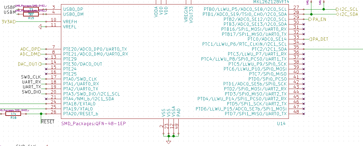
Kinetis KL26Z128VFT4
I wanted to have a microcontroller with a USB interface, so that it would be easy to interface with the PC doing the heavy processing. Integrated ADC and DAC would also be nice to save some board space and money.
The cheapest microcontroller having all these was Freescale Kinetis KL26Z128VFT4. It has an ARM Cortex-M0+ core that can be clocked at 48 MHz. It costs 3.4€, has USB, 16-bit ADC and 12-bit DAC. Though, when you actually read the datasheet ADC only haves about 13 effective bits without the hardware averaging. It isn't a big downside, since even 13-bits is very good precision for this price. I didn't notice it before ordering the board, but there is another catch with this processor: it only supports USB 1.0. In theory full-speed USB 1.0 can transfer at 12 Mbits/s which would be enough, but in practice this is not reached and only about five sweeps of 1000 samples can be transferred in a second, which gives a transfer speed of about 10 kB/s.
Transfer speed can be almost doubled quite easily by compressing the transferred signal. Since the signal is smooth, difference between two consecutive samples is small. This makes it possible to only transfer the difference to the last sample in one byte. In some cases the difference doesn't fit in one byte, this can be worked around by using a special value (I used all ones) for byte, which is used to signal that two bytes long full sample value follows. In practice this works really well and difference overflows only a few times in full sweep and about ten 20 ms long sweeps of 1000 samples can be transferred in a second. I believe that with more software optimization slightly higher speeds could be reached, but 10 sweeps per seconds works well enough that I haven't bothered yet.
From the software perspective this was very interesting processor. Kinetis offers a Processor Expert tool that can generate the driver code for the peripherals automatically. This makes configuring clocks, ADC, I2C and all other peripherals much easier and it works really well also in practice. There are some things that it doesn't support, for example changing the timer speed at runtime is not possible. Still, it's always possible to use the registers directly to implement the missing functionality.
I had much difficulties in programming this board, programming would succeed only very rarely and most of the time programmer would either fail to recognize the processor or fail to write to the flash. I even managed to brick one microcontroller so that it couldn't be programmed anymore. The cause turned out to be that this processor requires capacitance at reset pin. I couldn't find a note about this on the datasheet, but without it programming is not reliable. When looking at the reset line with the scope it seems that processor will generate a sawtooth signal on it. It seems that without the capacitor processor will reset itself too quickly for the programmer to connect. After adding a 100 nF capacitor to the reset pin everything started to work reliably.
RF portion
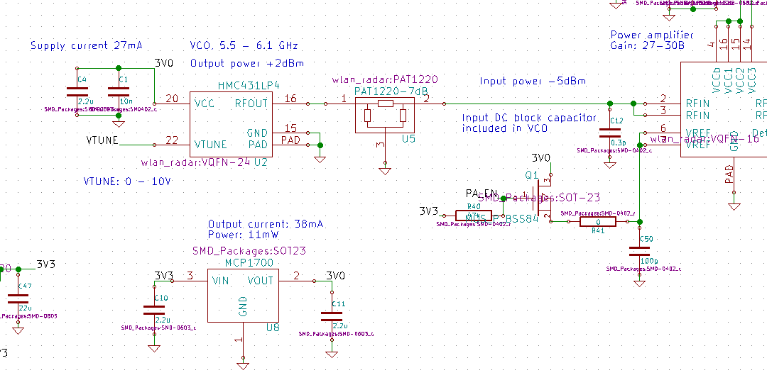
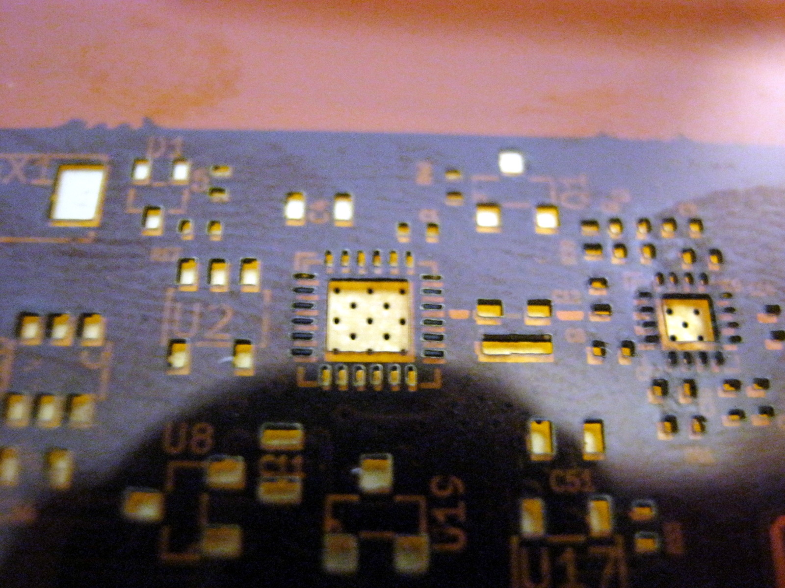
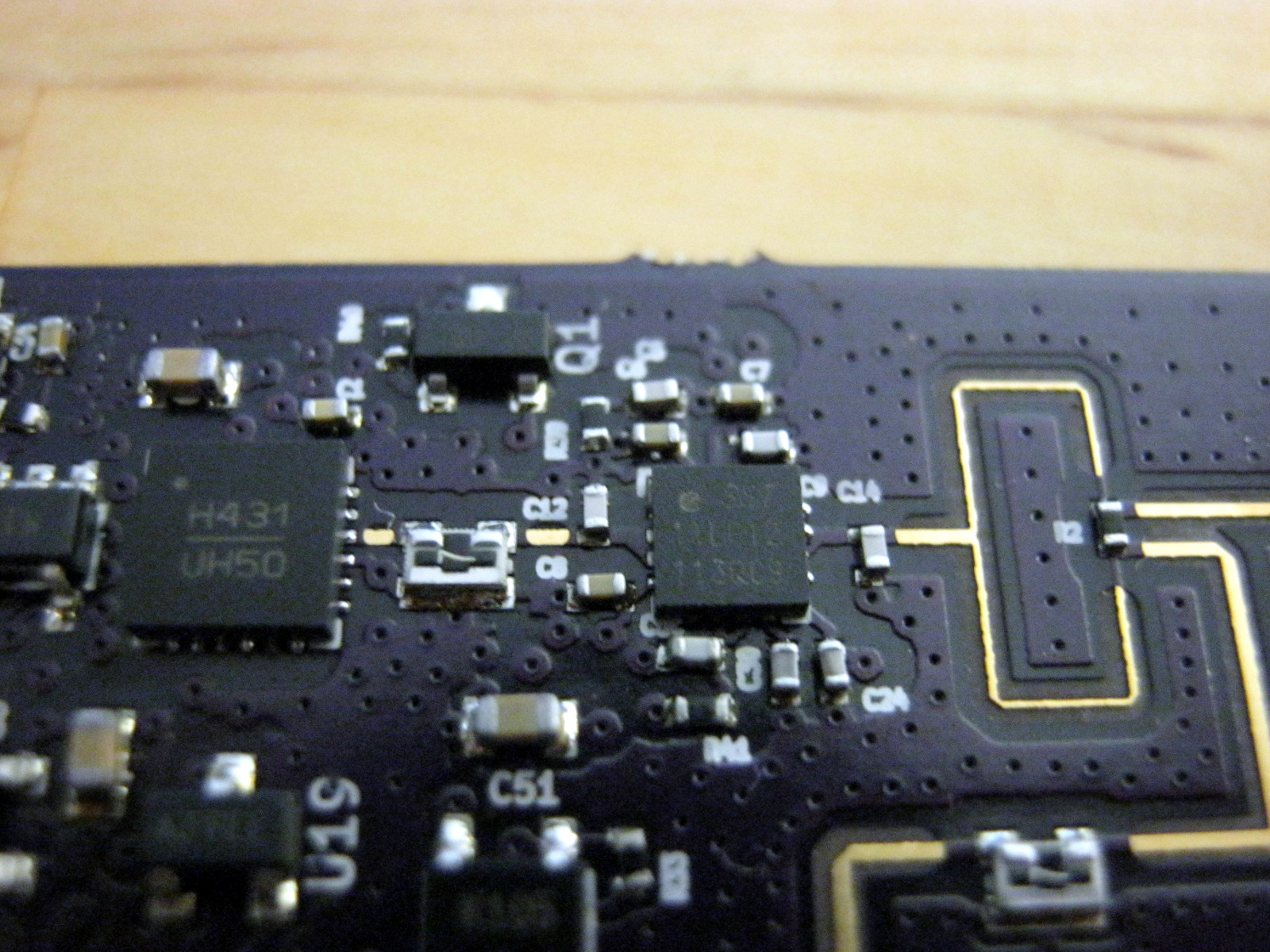
VCO and PA input
RF signal is generated by the voltage controlled oscillator (VCO), which tuning voltage is generated by the microcontroller. Output power of the VCO is 2 dBm, but because this power would be too much for the power amplifier attenuator needs to be places before the PA to attenuate the input signal so that it won't saturate the amplifier.
Discrete microwave frequency VCOs don't seem to be very common components and selection is very limited. VCO is the most expensive component in the whole radar costing 17€ a piece.
In the picture you can also see a MOSFET that allows the PA to be switched off by cutting of the bias voltage to it. 0 ohm resistor was put there to allow replacing it with a bigger resistor to drop the bias voltage if needed.
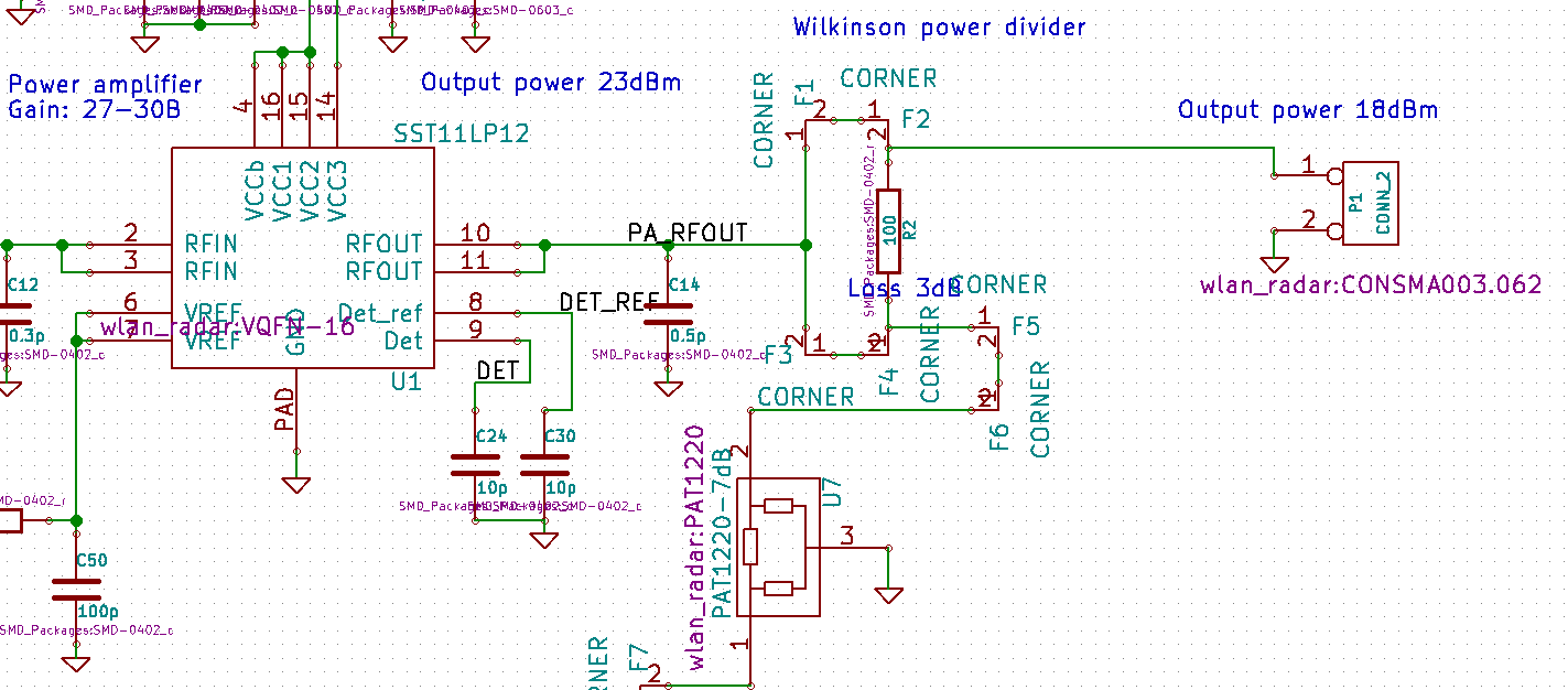
PA and power divider
The reason I chose to use 5 – 6 GHz band was because there is a band reserved for radars around 5.8 GHz and this range overlaps with 5 GHz WLAN. Since wifi components are very common, there are many different cheap choices for the power amplifier. PA I chose to use is SST11LP12 which is a cheap WLAN PA costing 1.5€. There would haven been cheaper PAs, but their datasheets were so short on the details that I didn't dare to use them.
PA is the component using most of the power on the board. Supply current is about 400mA from 3.3V. Since this is supposed to be a somewhat portable device and I don't want to include big batteries the power and communication is done over the USB. Maximum current draw of the USB device is 0.5A from 5V. This means that the PA uses about half of the available power. Since other components don't use nearly as much there shouldn't be a problem with USB powered operation.
PA amplifies the -2 dBm signal from the VCO to 21 – 23 dBm (0.1 – 0.2 W) signal depending on the frequency. Output signal then goes to the Wilkinson power divider, which divides the output to the transmitting antenna and the mixers input port. Since full divider output would be too much for the mixer a 7 dB attenuator is added before the mixer to attenuate the input signal to more manageable level.
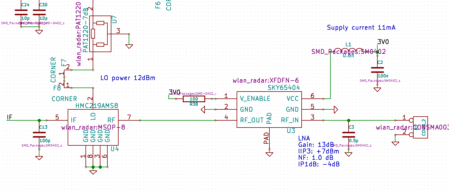
LNA and mixer
Radiated power is reflected from the target, captured by the receiving antenna, amplified by the low noise amplifier and then mixed with the PA output signal. LNA is also meant for the 5 GHz WLAN. It has a very low noise figure while also being incredibly cheap costing only 1.1€ at small quantities.
Amplified received signal is then passed to the mixers RF port, where it's mixer multiplies the PA signal and the received signal. IF port of the mixer then outputs two frequencies: difference of the input frequencies and the sum of the input frequencies. Sum frequency is over 10 GHz which exceeds to mixer output frequency and doesn't need to be worried about. Difference signal is the wanted result signal and it has a frequency of about 100 Hz to 10 kHz.
Baseband
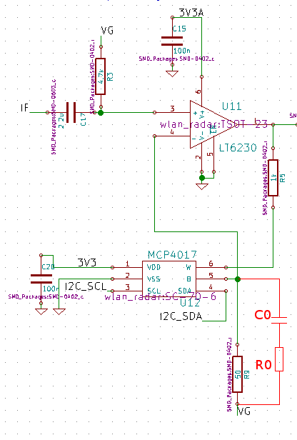
Variable gain amplifier
After the mixer output signal has a very small amplitude in about microvolt range and must be first amplified before filtering can be done. First amplifier uses LT6230 low noise op-amp in a non-inverting amplifier connection. MCP4017 is a I2C controlled variable resistor and varying it's resistance varies the gain of the amplifier. Gain is \(1+\frac{\text{R5}+\text{R(MCP4017)}}{\text{R9}}\).
Input signal is has some small DC offset that depends on the antenna to antenna coupling, but it should be around zero volts. Since I wanted to do this as cheap as possible I chose not to use dual supplies for the amplifiers. This means that signals DC offset needs to be rebalanced to 1.65V which is half of the op-amps supply voltage. Rebalancing is done with the capacitor C17 that blocks the DC voltage and resistor R3 which is connected to the 1.65V setting the signal DC level.
This works, but is not a very good solution. Resistor attenuates the signal and increases the noise at the input. In hindsight using two supplies would have been a better solution without increasing the cost by more than few euros.
DC balancing has also another issue: Since the balancing is done with a resistor the DC voltage at the input won't be exactly 1.65V. Amplifier has a high gain and it will also amplify the DC offset causing the output voltage DC offset to be off.
I noticed the issue before ordering the boards, but my solution of adding another DC blocking capacitor after the filter is not really a good solution since it doesn't fix the bad balance after the first amplifier. A better solution is to make the gain frequency dependent by adding a series connection of capacitor and resistor (R0 and C0 in the picture) in parallel with R9. DC won't flow through the capacitor and the gain is set by the R9. AC will flow through the capacitor and gain is set by the parallel combination of R9 and the resistor R0. I found that setting R9 to 1.5k and adding 44 uF capacitor and 50 ohm resistor worked well. This solution is not without downsides, R9 contributes most of the noise in the amplifier and increasing it will also increase the noise. It doesn't matter much though, since turns out that due to bad antennas gain can't be turned big enough for it to reach the noise floor.
Antialiasing filter
Because signal is going to be sampled by the ADC, filtering is needed to ensure that highest frequency of the signal is less than half of the sampling frequency, so that aliasing doesn't occur. Filter itself is the same as the one used on the MIT coffee can radar. Cutoff frequency is 15 kHz, but it could have been higher since the microcontroller can sample at least at 200 kHz. In practice it doesn't matter since range of the radar is not enough to generate a 15 kHz signal.
Filter is also not very good. It's a low pass filter, but since higher frequencies are generated by the targets that are farther away filters gain should increases with the frequency until the cutoff frequency. This way the weak higher frequency signals are amplified more and the dynamic range of the radar increases.
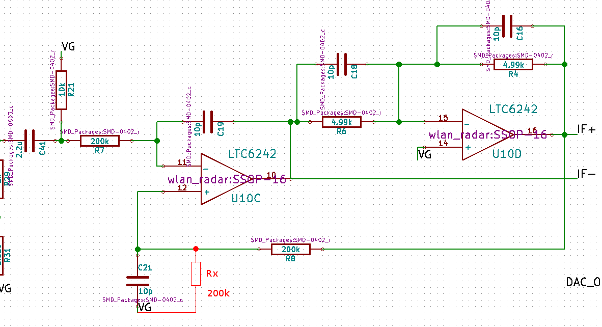
Single ended to differential conversion circuit
Using a ADC with differential input gives a better resolution than using a single ended input with the microcontroller that I'm using. The circuit above is straight from the LTC6242 datasheet and it will convert the single ended signal from the filter to differential signal for the ADC.
This circuit also had some unexpected problems. LTC6242 is rail-to-rail op-amp, but when I tested the circuit output saturated already at 2.6V even though operating voltage is 3.3V. Cause for this turned out to be the common mode voltage range of the inputs. 2.6V is the maximum voltage that should be applied to inputs and higher voltage than that will saturate the inputs and the output responds as if the input voltage was 2.6V.
Fix for this isn't too complex. Some gain needs to be added to the circuit so that the 2.6V input generates 3.3V output without any inputs voltage exceeding 2.6V. This is possible by adding a resistor Rx in parallel with C21. This attenuated feedback signal to the first op-amp which causes its output to increase output voltage so that the feedback voltage at negative input equals the input signal at positive input. Full voltage of the first op-amps output won't be applied to the second op-amp and the circuit will work correctly with full output swing.
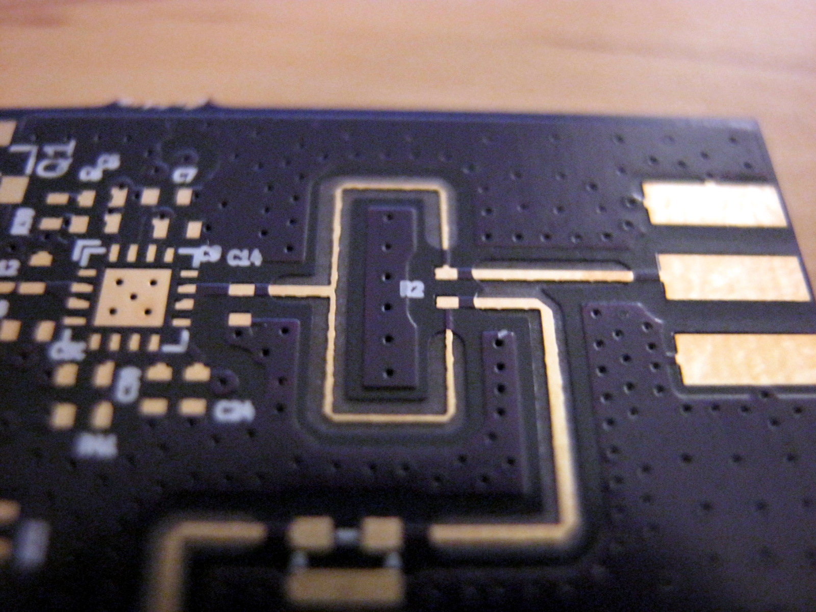
Power splitter
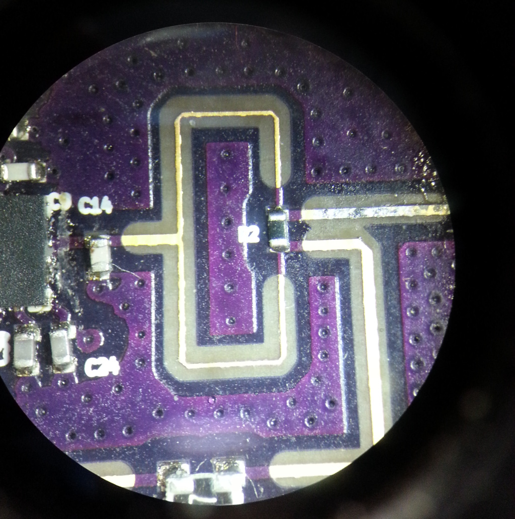
Power splitter is a Wilkinson divider. It's lossless divider with good isolation between the ports, but it is frequency dependent. If the signal is too far off from the design frequency isolation between the ports suffers. Frequency range that radar uses is not too big for this to matter too much and it works fine. One disadvantage in this application is the equal division of the power. We would like most of the power to go to the transmission antenna and only a little bit to the mixer. With equal division there needs to be an attenuator before the mixer to make decrease the input power. This is a wasted power that should be used in transmission. More complicated power splitter would add too much board area to be worth it, even the simple Wilkinson splitter uses large amount of the board compared to how many components could be fit into the space it uses.
I would have liked to use smooth bends in the splitter since they are simple to design, but Kicad doesn't support them. So instead I had to use 90 degree mitered corners. Mitered corner is just a bend with a cutout on the corner which negates the impedance change from the bend. They are very often used in microwave circuits since they don't reflect the signal and can be fit into smaller space than smooth bends.
Solder mask is also removed from the top of the traces so that it doesn't affect the impedance. It also has a side effect of making the traces look much cooler since the beautiful gold plating is visible. Large number of vias are required to connect top and bottom ground planes together. Wavelength at 6 GHz is about 36 mm, distance between the vias needs to be much smaller than this so that there isn't potential differences in the ground planes. A common rule of thumb is that the distance between vias should be 1/20 of the wave length. Since adding more vias doesn't cost anything I were generous in placing them and the distance between vias is about 1mm around the RF traces.
First version I designed used the usual design equations: Impedance of two divider traces is \(\sqrt{2}\times 50 \approx 71~\Omega\) and the length is quarter of the wavelength, which equals about 8mm.
Since I had a access to CST microwave studio, I decided to simulate the divider with it. CST has a handy feature that allows importing the gerber files so the simulation model dimensions are exactly as drawn in KiCad.
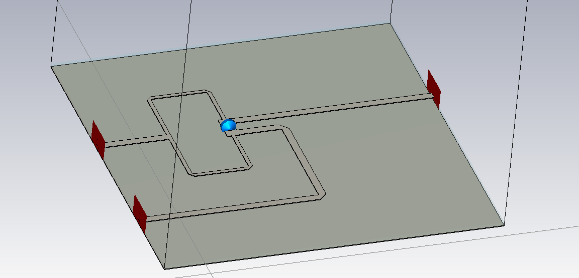
Power divider modeled in CST. Blue cylinder is 100 ohm resistor and red planes are waveguide ports.
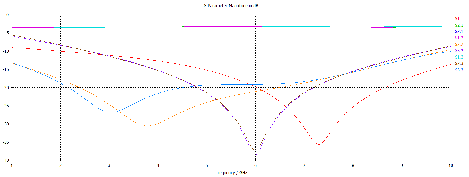
Divider was designed to have a center frequency of 5.5 GHz, but according to the CST it's working best at 6 GHz. Adding 1.2 mm more length shifts the working frequency to 5.5 GHz. I guess the difference is caused by the fact that I calculated the trace length from the branch to the center of resistor pad, but I believe length of the trace should be calculated from the branch to the center of the resistor.
From the low S11, -35 dB at best, it can be seen that the mitered bends are working and only a minimal amount of power is reflected back to the input. Though even with a straight 90 degree bends without miters reflections at these frequencies are most likely going to be minimal since wavelength of the signal is much bigger than the corners.
S21, gain from PA to transmitting antenna is -3.3 dB. Ideally it would be -3 dB, which equals even split of power with nothing being wasted, but especially substrate losses consume some of the power. 0.3 dB extra loss is still a very good figure.
With the adjusted trace lengths port isolation is below -20 dB at all usable frequencies (5.3 GHz to 6.3 GHz).
SMA connector interface
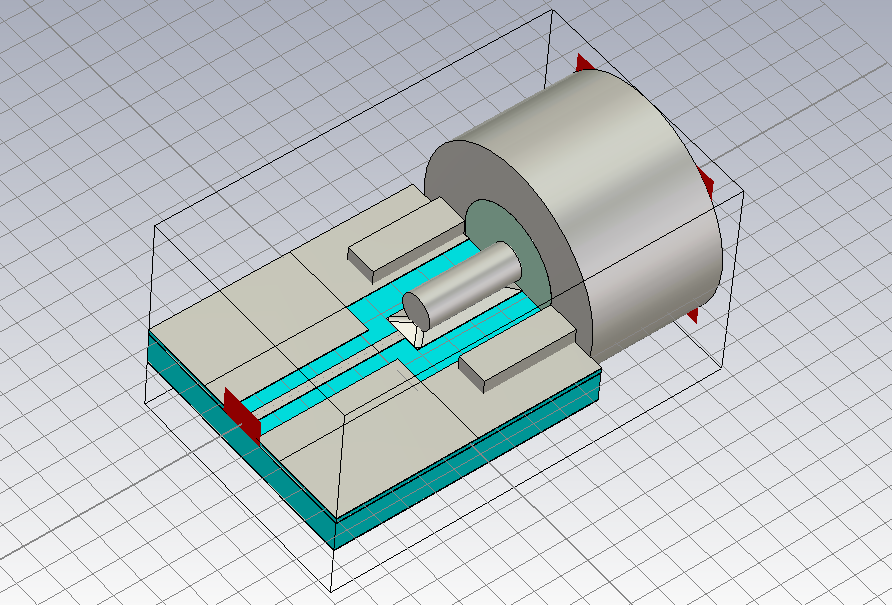
SMA connector modeled in CST
With ordinary low frequency design something as simple as connector doesn't really require any attention. However, things are different with RF frequencies. To minimize the loss in microstrip to coaxial cable transition I decided to simulate also this interface. The potential issue with the connector is that the 1.3 mm center conductor is much bigger than the 0.35 mm microstrip that should connect to it. Since connector pin needs few millimeter solder pad to solder the pin, the pad itself works as a microstrip and since it's so wide it has a very low impedance and there is a significant impedance discontinuity between the microstrip and coaxial cable which reflects the power back.
There are connectors that are more suitable for these track widths, but these are the cheapest SMA connectors and even they are quite expensive costing 3€ a piece. Better ones would have costed about 10€ a piece, which would have been a significant part of the total cost.
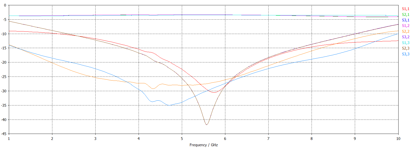
Simulation confirms that the there is an issue. S11 is -3 dB at 6 GHz, which means that half of the power goes to antenna and other half is reflected back. But this doesn't mean that this connector cannot be used, it only requires some changes to interface. Issue is that the solder pad works as a microstrip and it has a wrong impedance. Making it thinner would solve the problem, but it's not possible or connector can't be soldered. The other solution is to make a cutout to the ground plane. Because impedance of the microstrip depends on the distance to the ground plane below it, making a cutout to the ground plane below the pad will raise its impedance and eliminate the impedance discontinuity.
After few simulations turns out that the optimal cutout is 3.7x2.6 mm and with it the S11 is -22 dB, so hardly any power (0.6%) is reflected back.

Ground plane cutout.

Soldering the board
Beautiful purple PCBs from OSH Parks.
Some roughness can be seen on the thin power divider 71 ohm trace edges. It's not very good for performance since width of the trace affects its impedance. Roughness is still low enough that the effect to the impedance should be minimal.
Paste for the QFNs can be applied by hand, but I'd rather avoid it if possible. Using stencil just makes applying the solder paste so much easier and saves so much time that it makes sense to order a stencil even when making a single board since they are so cheap.
A very good spread of the paste. There was a slight misalignment of the stencil, but it isn't big enough to matter.
I could really use microscope with some of the smallest components, but I managed to place all the components even without one. 0402 passives are still kind of pain to use, but they save board space and are required for RF reasons in some places.
After five minutes in the oven paste has reflowed and components are soldered. Soldering with the reflow oven is just so good that I wonder how I once managed without one. Solder joint quality is just so much better than manually soldered and oven gets the job done much faster.

For the smallest board (and cheapest price) both sides of the board need to be used. I planned on not ordering a stencil for the backside so there are only few passive components which I applied the solder paste manually.
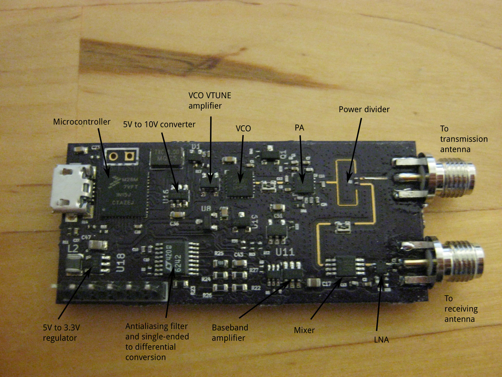
Finally above is a picture with the different components labeled. Unlabeled components on the center are: 3.3V regulator for analog components, 3.0V regulator for VCO and LNA and op-amp to for generating 1.65V virtual ground for the baseband filter.
VCO VTUNE amplifier is needed to amplify 3.3V DAC output signal from microcontroller to 10V.
Testing the board
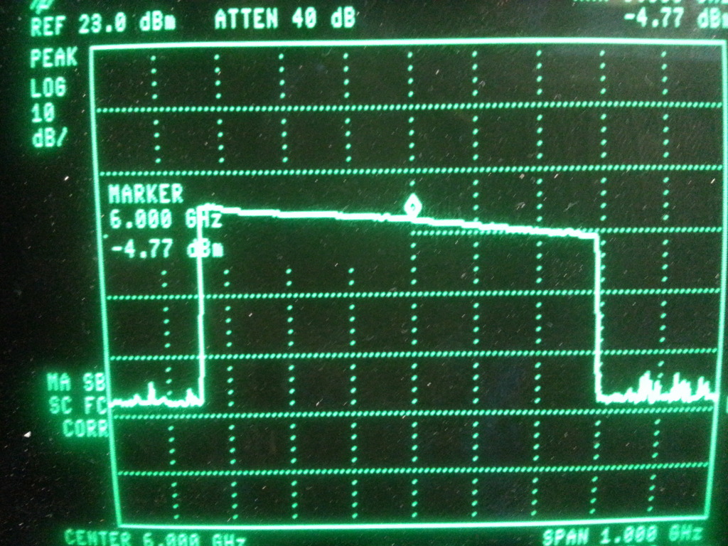
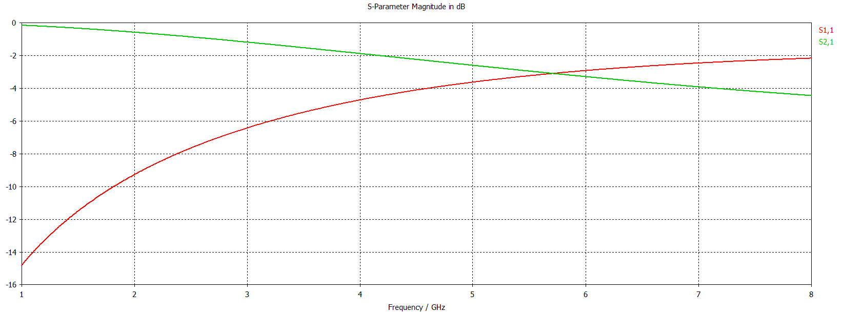
Above is the spectrum analyzer output when radar is VCOs tuning voltage is swept full range from 0 to 10V. Output frequency goes from 5.6 GHz to 6.3 GHz. Since there is a 20 dB attenuator at the output, real output power is 15 dBm. This includes the loss in the 1m SMA cable which should be around 1 dB at these frequencies.
Output power is not quite even and drops actually 6 dB over the range. This is expected and follows the specifications in the PA datasheet. Maximum gain is achieved already at 4.0 GHz and it drops by about 10 dB at 6 GHz. This amount of gain unevenness is not a problem since sweep bandwidth is around 100 MHz and drop over this bandwidth is low.
Theoretically input power of the PA is -5 dBm and gain is about 27 dB at 6 GHz, so the output power should be 22 dBm. Since the power divider has simulated loss of 3.3 dB the output power should be 18.7 dBm minus the unknown loss in the cable. Measured power is not quite the calculated one, but it's close enough to say that the PA and divider are working as designed.
Antennas
With the board done it's time to make the antennas. Usually radars use very directional horn antennas. Directionality of the beam is important so that only signal from the target is picked up instead of the surroundings. Besides the directionality radar antenna should have low sidebands so that antenna to antenna coupling is low and it doesn't pick up reflected signals from behind and sides of the radar. Also the antennas should not reflect the power back but instead do their job and radiate it.
Maybe one of the best antennas would be a pyramidal horn antenna. It can fulfill all the specifications, except that manufacturing is expensive. I didn't want to spend too much money in making a very good antenna when I wasn't sure if the radar board would work. So instead I decided to first make cheap and crappy antennas to test the board and maybe then manufacture proper antennas.
So I decided to make antennas out of cans. Can antennas are more commonly known as cantennas. Problem with most of the cans is that they are too big for 6 GHz range. 33 cl soda can would be good but they are made out of aluminium which I don't have equipment to solder. Most promising cans I found were two quite small cans originally containing canned pears.
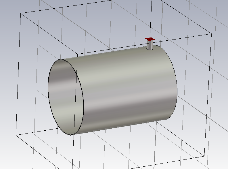
Model of the cantenna in CST.
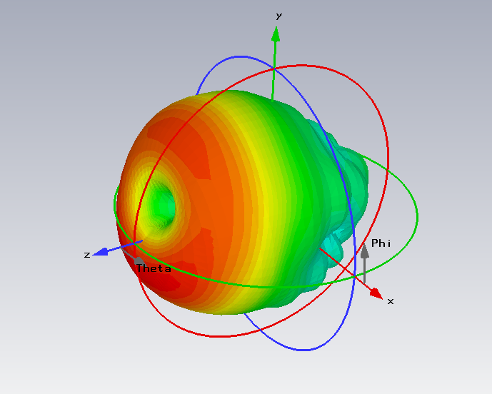
Simulated farfield directivity pattern.
The only free parameters with the cantenna design is the location of the SMA connector and length and the diameter of the SMA connector center wire. Even though I tried to optimize them as best I could, not surprisingly performance of the cantennas is really bad. Beam width is 100 degrees, which is really wide for a radar antenna. Simulated radiation pattern is also quite weird, there is a hole right in the center of the main beam and no matter how I adjusted the feed position, feed line length or its diameter I couldn't get rid of the hole without sacrificing radiation efficiency.
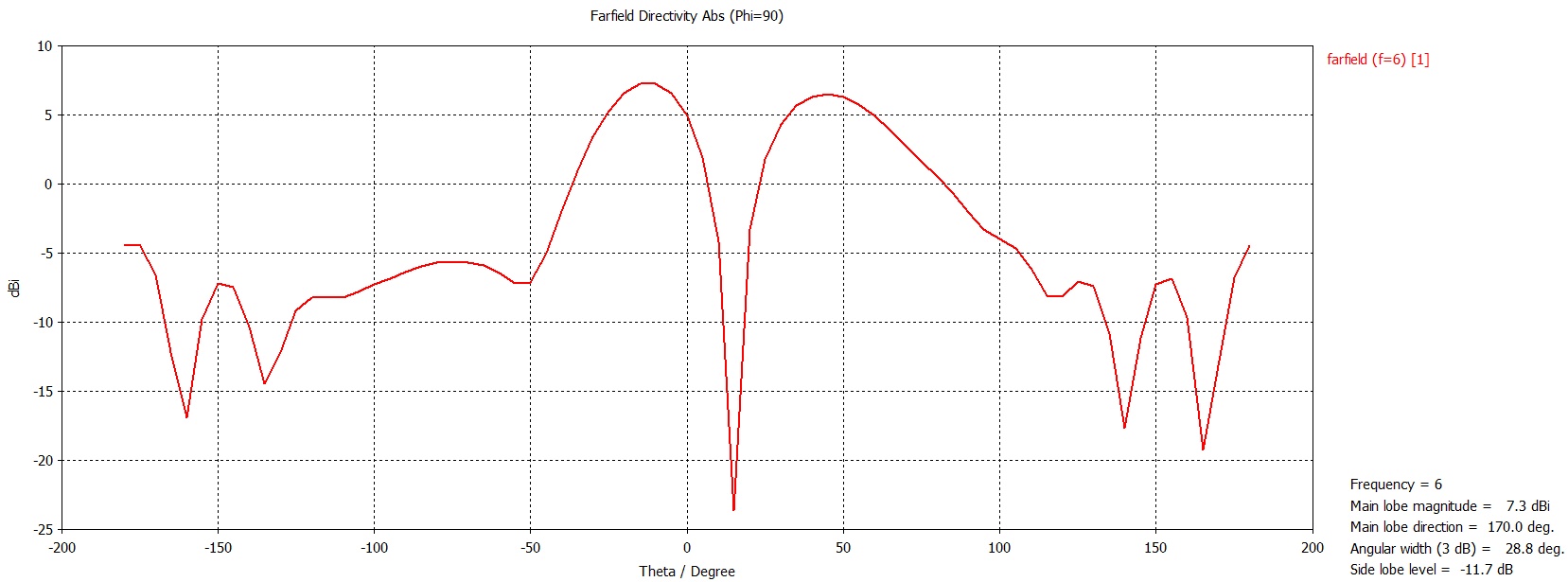
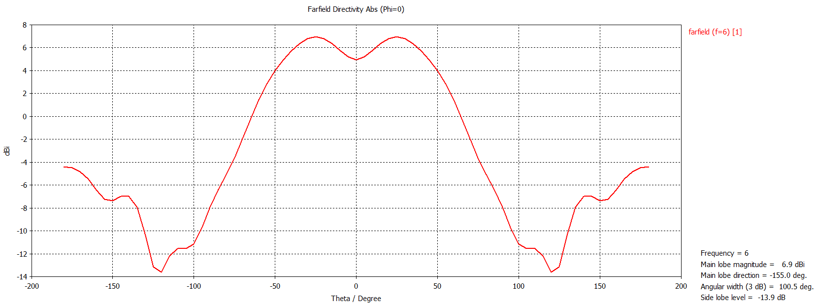
As can be seen from the above, the hole is pretty deep. It's a pretty bad antenna but it should be enough to test if the radar works.
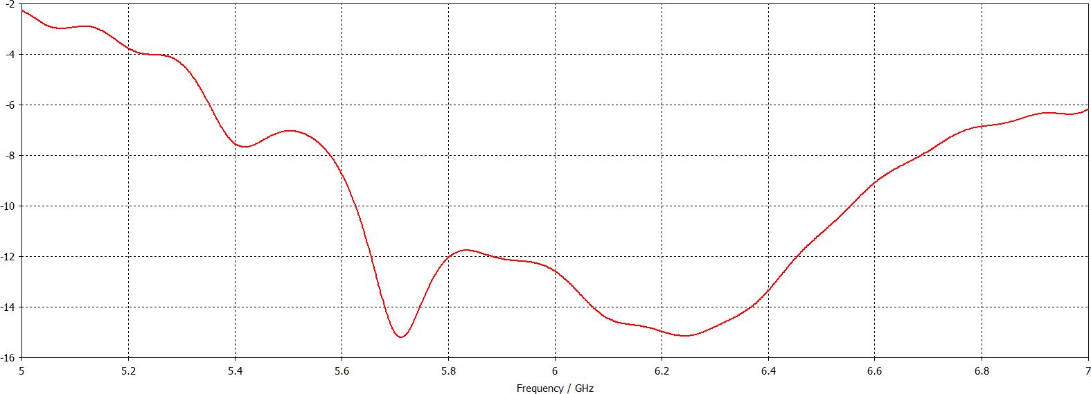
Input reflection is decent, anything below -10 dB should be fine.
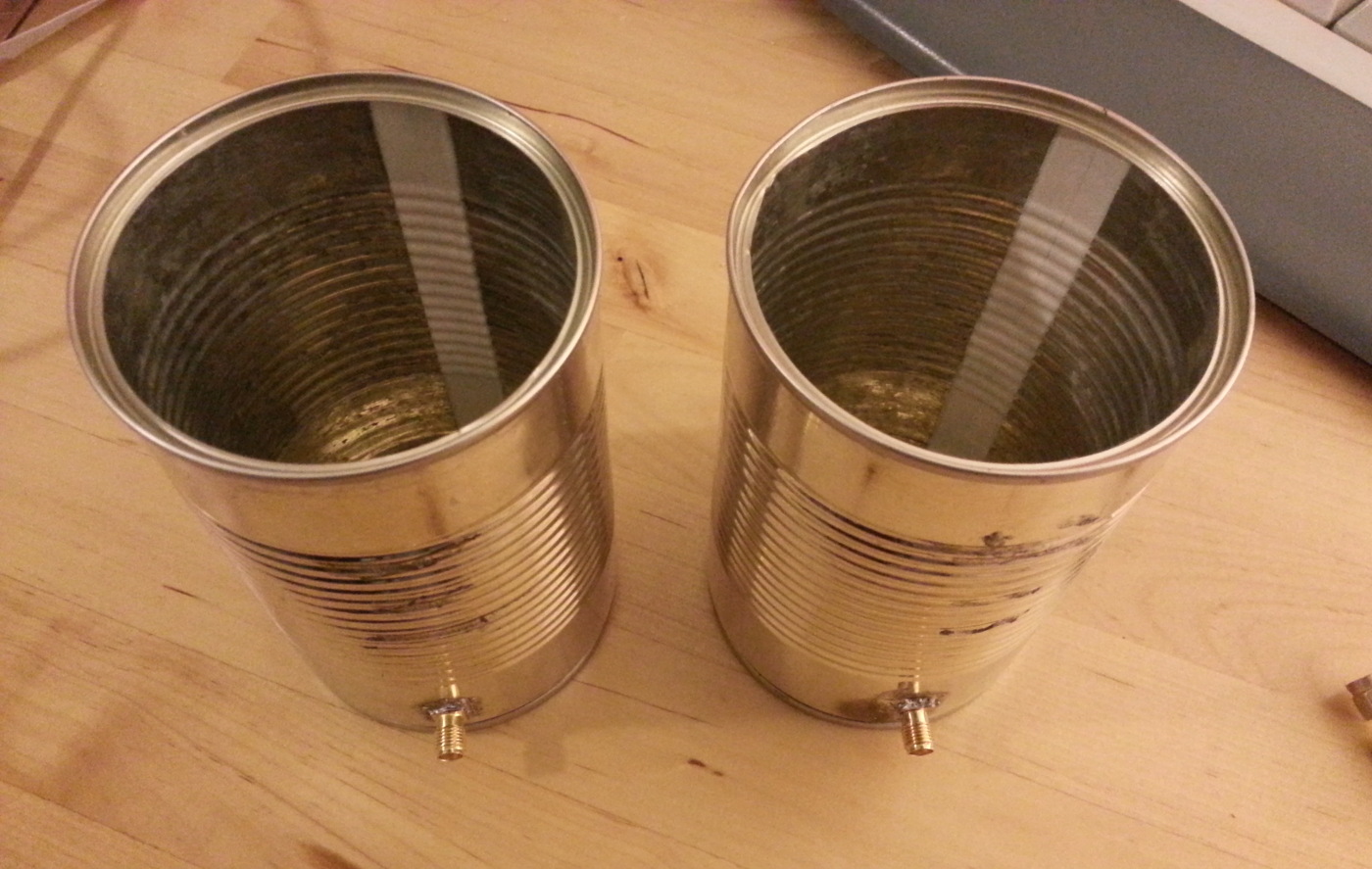
Finished cantennas.
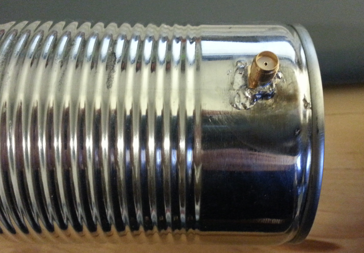
Closeup of the SMA connector.
Best way to solder the SMA connector is to first remove the teflon insulator and just solder the shell first. It's easier to position if the teflon piece is inserted from the wrong side so that it comes out to the inside of the can. Then the teflon piece will center the shell into the hole, which makes soldering it much easier. After soldering the shell feed wire needs to be soldered to the center conductor of the SMA connector. This is also easier to solder with the teflon piece removed. After soldering the feed the teflon piece can be pushed back from the outside.
I was first worried if the soldering iron would have enough power to heat the can hot enough, but there weren't any difficulties in soldering the connector with a regular soldering iron and a regular solder wire.
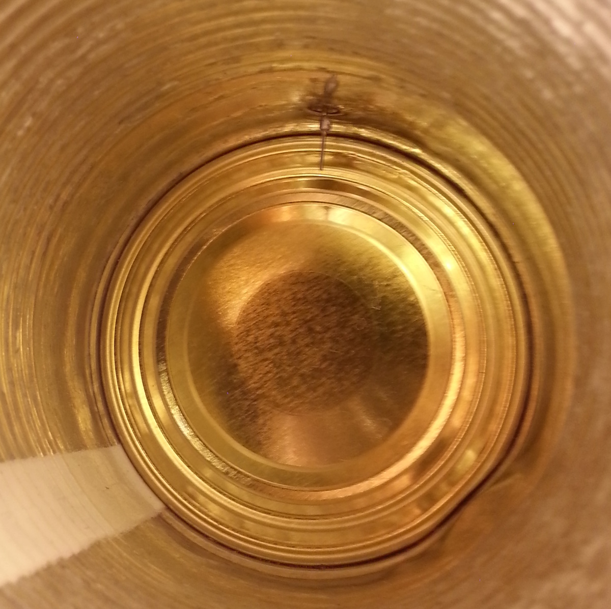
Inside view showing the feed.
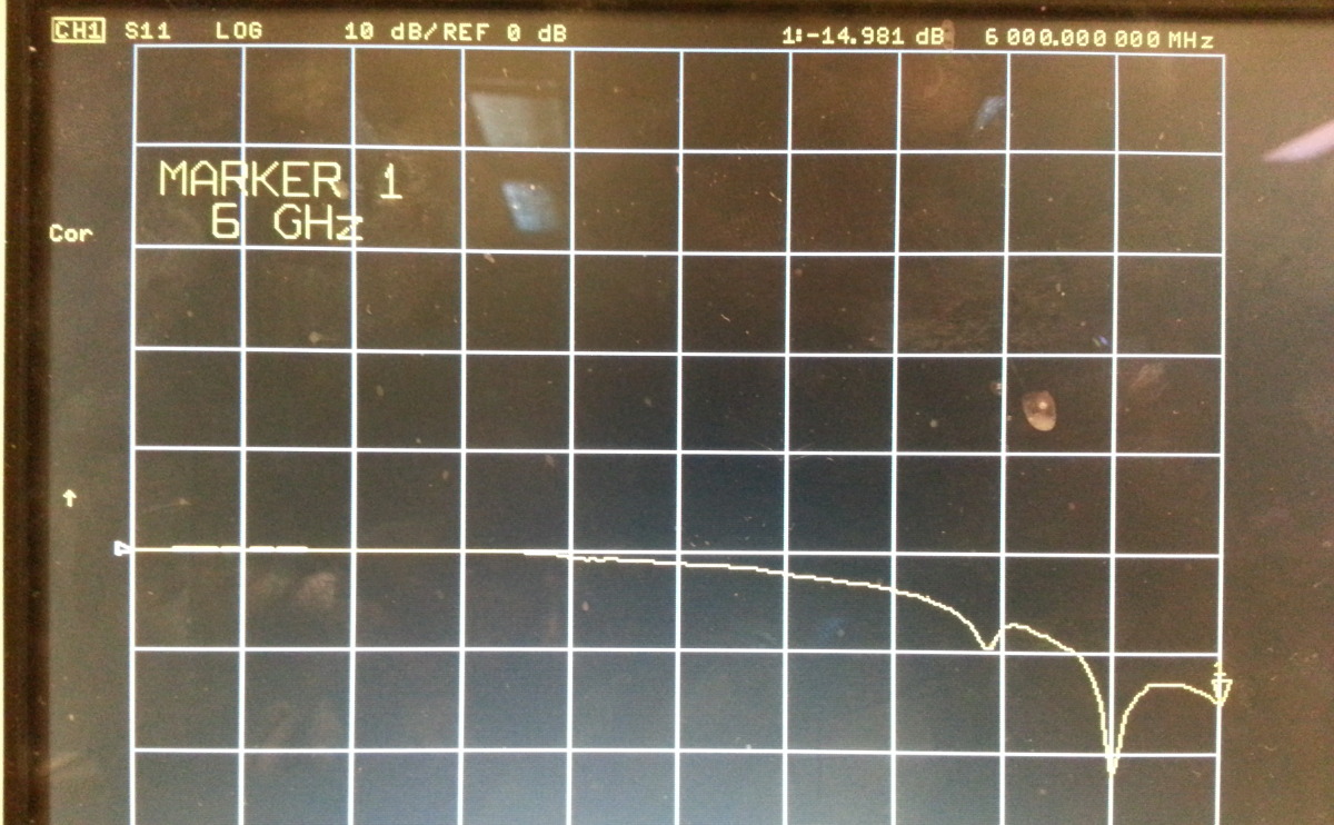
I also measured the S11 of the real antenna using network analyzer. It had a maximum frequency of 6 GHz so it was just barely enough. Measured S11 is -15 dB at 6 GHz, which is actually better than a simulated value. This might be the first time that something works better in real life than simulations. Both of the antennas have pretty much identical S11, so manufacturing tolerances probably can't be blamed. Reason is probably the caused by the simplistic model which didn't include the ripples in the can. Those would have been too time consuming to make, so I just modeled the antenna with smooth walls. Shape of the S11 still agrees closely to the simulated shape suggesting that the simulations are not too inaccurate.

Finally I taped the antennas to a supporting plate and connected the radar board.
Outside testing
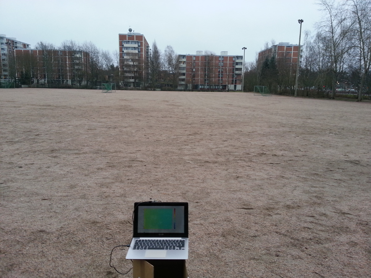
Above is a football field where I tested the radar. I used a carboard box to raise the antennas from the ground. In the picture radar is behind the PC.
Usually radars have very directional antennas so that they can be pointed accurately at the target without too much reflections coming from the surroundings. Since the antennas that I'm using have a beam width of about 100 degrees, radar is going to pick up a lot of reflected signals, also called clutter, from the surroundings.
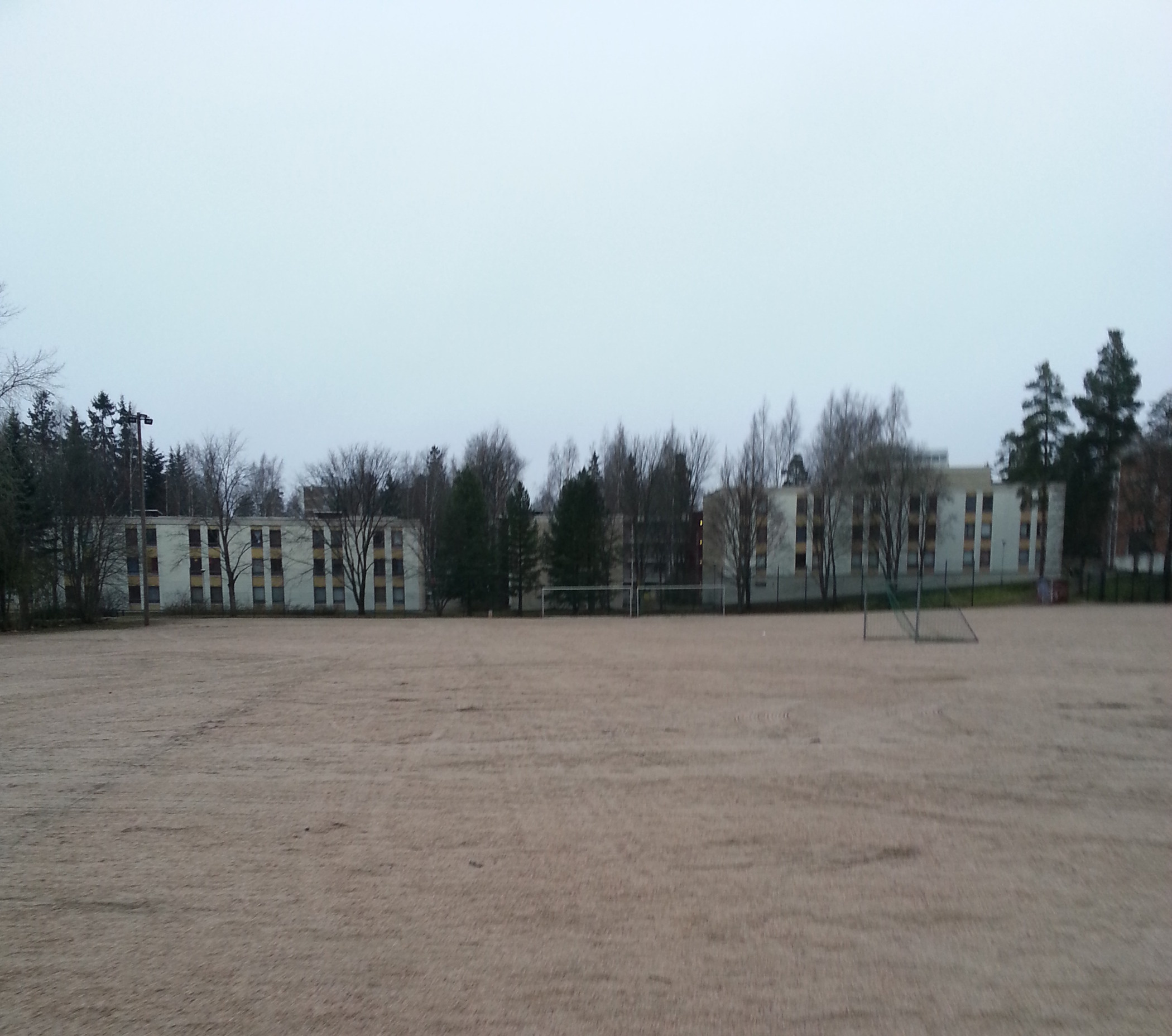
Above is the view from the other side. Box under the radar can be seen at the middle, but radar isn't really visible at this distance.
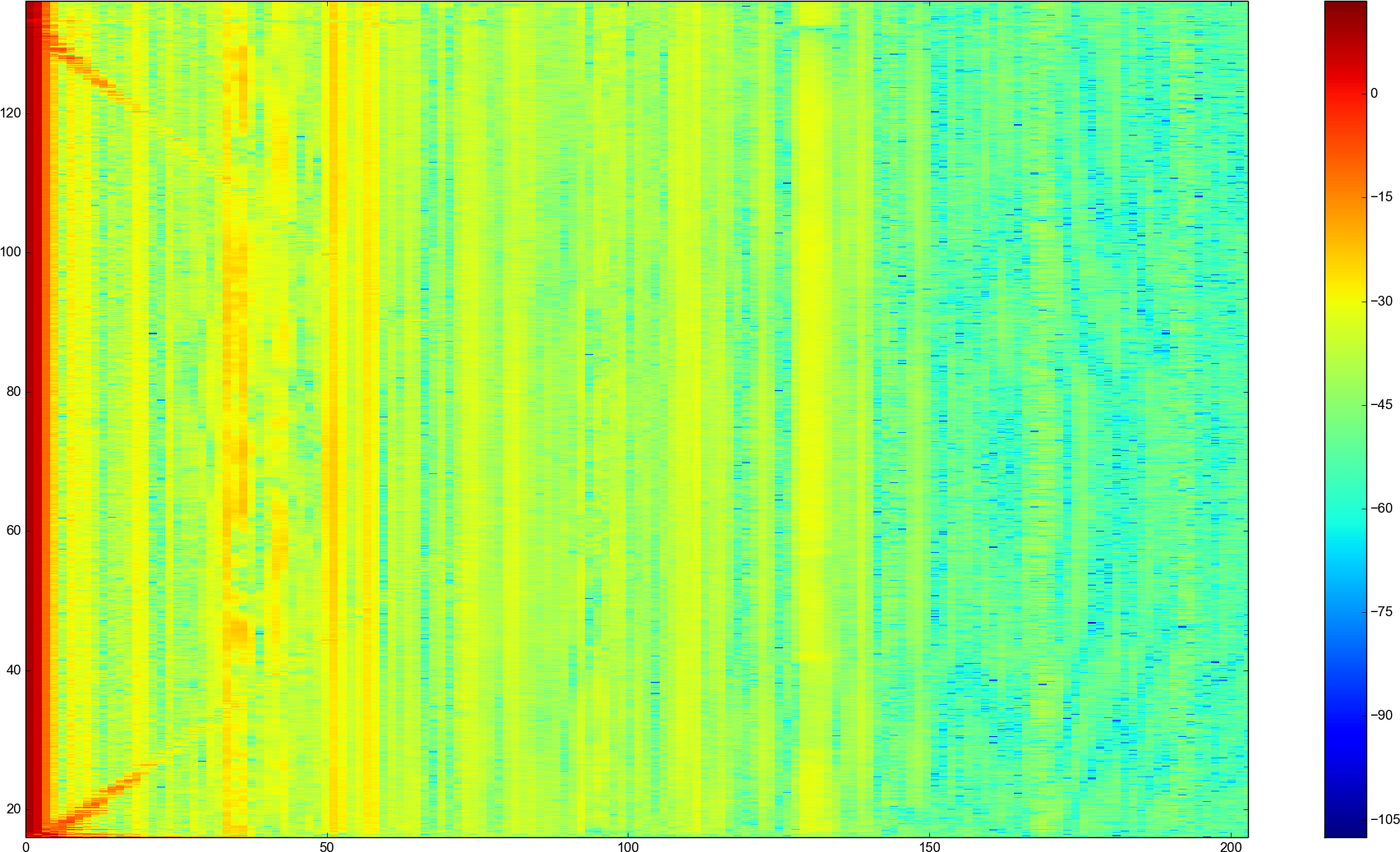
Above is the processed signal plotted as time in seconds on y-axis and range on x-axis. Colors are the power of the detected frequency referenced to some arbitrary value.
There's a quite lot of clutter in the foreground from the trees at the sides. Some of the clutter is also caused by the reflections from sides and behind of the radar via sidebands of the antennas. Around 50 m clutter from the goals in the middle of the field can be seen clearly and at around 130 m is clutter coming from the buildings at the background. It's quite hard to see, but especially at the foreground a diagonal line of my path can be seen.
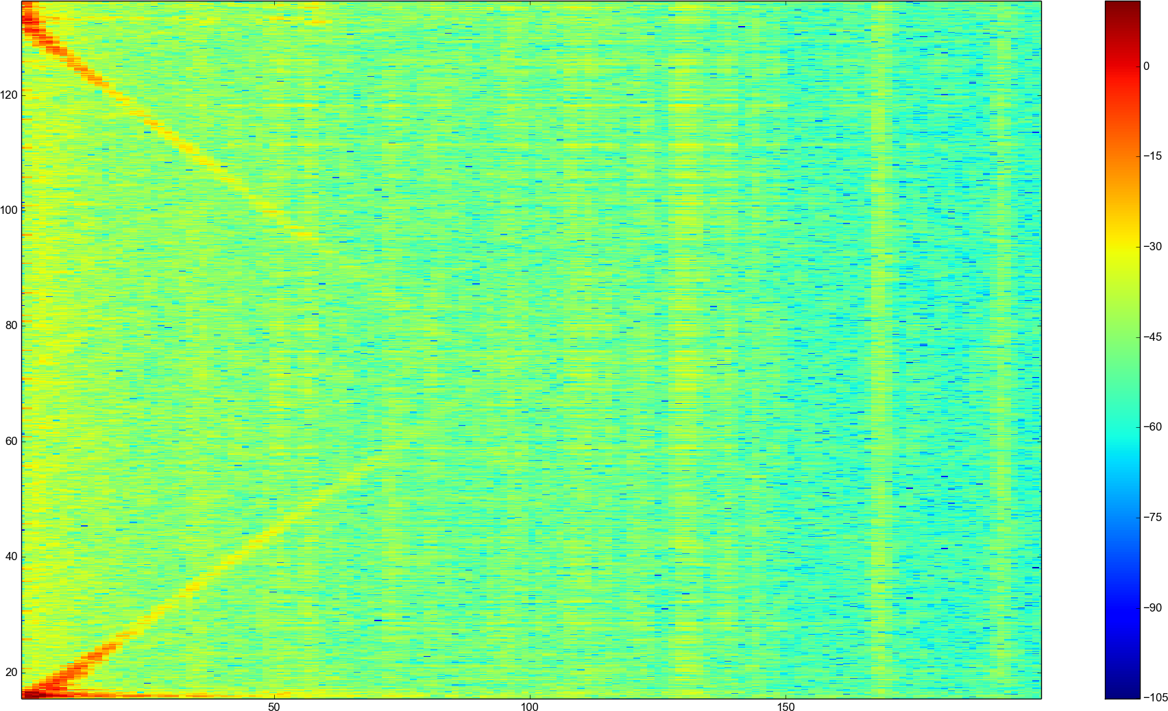
After subtracting the previous pulse from the current one all the stationary clutter is cancelled and suddenly things are much more clearer. Signal to noise ratio is about 15 dB at 50 m and goes to zero near 90 m. There is still quite a lot of noise due to clutter not being completely canceled. For example wind moving trees and inaccurate sampling causes the consecutive pulses to not be completely identical and there is some clutter left even after the subtraction.
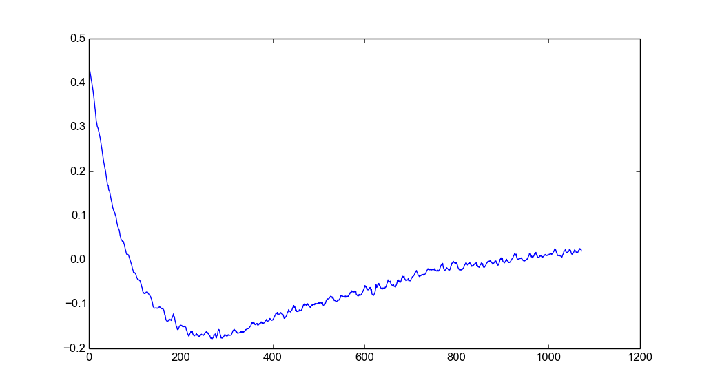
Capture of one sweep. ADC range is scaled from -0.5 to 0.5.
Above is one of the captured waveforms and it's clear that everything doesn't seem to be right. There is a very big peak at the beginning of the sweep which limits the maximum gain of the automatic gain controller to about one third of the maximum gain. If the peak and the low frequency signals wouldn't exist, the gain could be increased which would also improve range of the radar.
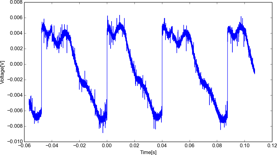
Mixer output captured with an oscilloscope.
Looking at the oscilloscope capture of the mixers output it's clear what the cause is. Low frequency high amplitude signals caused by the reflections close to the antenna cause very big discontinuity at the start of every sweep. Since this signal is AC coupled to the baseband, it will cause a decaying peak after passing through the capacitor. Fix would be to use better antennas.
So in summary the radar works and the range is not too bad, though it could be easily increased with better antennas and I thats what I'm going to start working on next.
All hardware design files, firmware and processing software is available at github