PIC16F84 is old 8-bit microprocessor made by Microchip. It was once very popular among the hobbyists, because of its low price. It was the first microprocessor I started to use so I thought it would be fun to try remaking it in VHDL. The source code is open source and can be found on my github.
I first started writing a single cycle design, but converted it to two-staged pipeline, because the real pic16f84 uses this kind of architecture. Two stages are fetch/decode and read/execute/writeback. For performance reasons it would be wise to have even more stages. With three stages separating the writeback to is own stage would increase the maximum clock frequency the most, but complicate the design and make some instruction take more time to complete in clock cycles than on the real version.
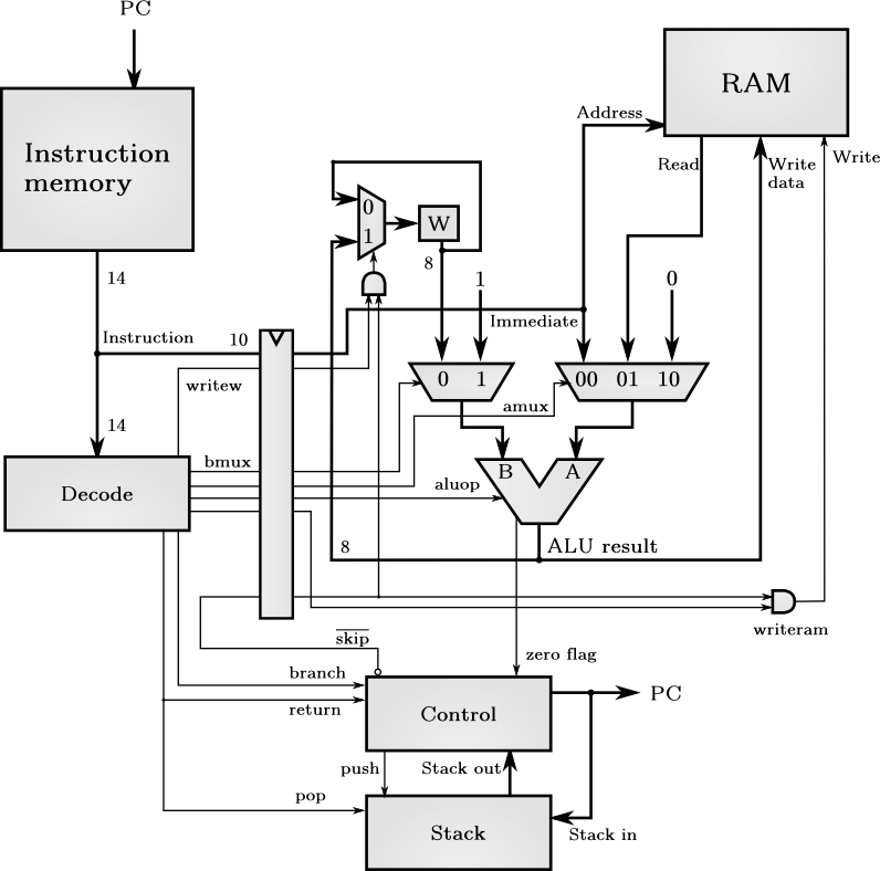
Simplified datapath and control signals. Signals not related to the program flow are removed.
PIC16F84 has very simple accumulator based architecture. There is only one accumulator register called W. Instructions are decoded to few control signals that control the multiplexers and other datapath elements. I don't know exactly how the microchips real version works, but I think it's very similar.
Executing the instruction start with fetching the instruction pointed by the program counter (PC) from the instruction RAM. Next it will be decoded to control signals that are used to control the datapath. Control signals go through a flip-flop that buffers them and allows decoding and executing two different instructions at the same time, better known as pipelining. Then the datapath reads RAM, executes the instruction and writes the result back if needed. This is the critical stage that limits the clock rate of the whole microprocessor. It would be advantageous to divide this pipeline stage to two or three seperate stages for higher clock frequency.
Control unit is responsible for stalling the exeuction state when needed, computing the new program counter and handling the interrupts. On call instruction or interrupt the current PC will be pushed on the stack and it will be popped from there on return instruction.
Control signals
| Signal | Function |
|---|---|
| amux | ALU B-port multiplexer control signal |
| bmux | ALU A-port multiplexer control signal |
| writew | W <= ALU result, when this is 1 |
| writeram | ALU result is written into memory location pointed by the current instruction |
| aluop | ALU operation, possible operations are: pass A-port, AND, OR, XOR, NOT A, A-B, A+B, A<<1, A>>1, set bit, test bit and swap nibbles of A (low and high 4 bytes) |
| branch | 1 if decoded instruction is call or goto |
| return | 1 if decoded instruction is return, retfie (return from interrupt) or retlw (return and set W to immediate) |
With these control signals we can implement all of the instructions. For example movlw instruction, that moves literal to W is implemented as writew <= '1', aluop <= Pass A and others zero. This moves the literal from instruction to ALU result and to the W register input.
bmux signal might seem weird, but we need constant 1 available to this port when incrementing or decrementing a memory location. This could be replaced with two new ALU operations, increment and decrement, but it would really synthese into very similar logic.
Constant 0 on the other ALU multiplexer is used for clear W and clear memory location instructions. Also instruction that moves W to RAM is implemented as adding zero to W and then writing the ALU result to RAM, this way we don't need an ALU operation that passes the port B to ALU result. This again reduces the number of ALU operations needed and makes the microprocessor a little bit faster.
Zero flag from ALU to control logic is used for conditional branches. This signal is 1 if ALU operation is zero. When the conditional branch is taken we need to discard the result of the next instruction that is currently on the decode stage. This is done by asserting the not skip signal, which forces the writew and writeram signals to be zero for the next clock cycle. The instruction is executed, but because the result is not written anywhere it doesn't matter.
Lessons learned
Pipelining can easily have some subtle errors. Like when writing to program counter register in the RAM it functions as a branch. Writing can be actually done directly to the right RAM location or indirectly through special pointer RAM location (FSR). Both need to be checked at the control logic to stall the execution state.
It is easier to use RAM that has asynchronous read, but block RAM in the FPGA has synchronous read. If asynchronous read RAM is required it must be implemented as distributed RAM. I converted my instruction RAM halfway through the design from asynchronous to synchronous,
1 2 3 4 5 6 7 8 9 | |
RAM with synchronous read. Moving the "d1 <= mem(to_integer(unsigned(a1))); " one line down would make the read asynchronous.
I have still implemented the data RAM as asyncrhonous read and I don't think it's possible to make it synchronous without adding pipeline stage. Address to read is calculated in ALU so the data read would be delayed to the next clock cycle.
Testing, you can never have too much of it. I started testing first by writing short programs and checking their output manually. This soon turned out to be too time consuming, because I would manually need to check outputs of the programs after making changes. Modifying programs to write results of the operations to output ports and using assert commands to test the correct values turned out to be much easier.
I have heard that some people generate random programs and compare the output to reference implementation written in behavioral VHDL or other language. It would be a very effective way to find bugs, but writing the reference implementation would take too much time.