Introduction
A while ago ordered a PCB where I made a mistake of connecting SD card to 1.8 V logic level I/O pins instead of the correct 3.3 V. As a result the SD card in that PCB didn't work. Otherwise the PCB was good and I didn't want to reorder the whole PCB to fix this one mistake as it would have cost over 500 EUR.

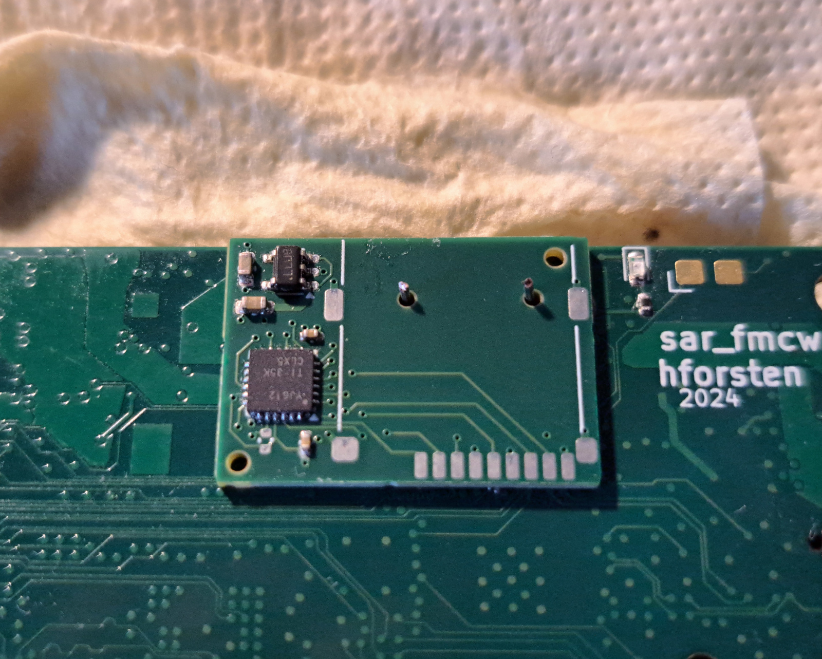
Bottom of the PCB and the incorrectly wired SD card connector pads.
I had placed the SD card connector on the bottom of the PCB without many components near it. The plan to fix it was to manufacture a small interposer PCB with 1.8 V to 3.3 V logic level translator, SD card connector, and matching pads on the bottom so that it can be soldered directly to the bigger PCB.
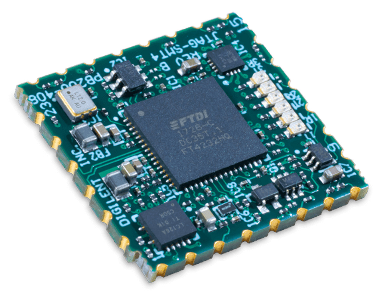
Example of commercially sold PCB with castellated holes meant to be directly soldered on bigger PCB.
Typically when soldering PCBs directly together castellated holes are used. They are plated holes that overlap the edge of the PCB such that half of the hole is routed out. This leaves nice plated edge to the PCB that is easy to solder.
However, the issue with using castellated holes in this case is that pitch of the SD card connector pads was only 1.1 mm which was too small for castellated holes for any low cost PCB manufacturer. Another issue is that since the SD card connector is at the edge of the PCB, the new interposer PCB would have needed to stick out a little to make room for the castellated holes.
The remaining option was to put SMD pads under the interposer PCB. With 4-layer PCB it would be possible to mount the new SD card connector directly over the old one and the level shifter could be next to the SD card connector. The drawback of this approach is that since the pads are under the PCB it's not possible to solder them with soldering iron and it would require using solder paste and hot air tool.
I did find some discussion if this was possible but I didn't find any actual results, which motivated me to write this post.
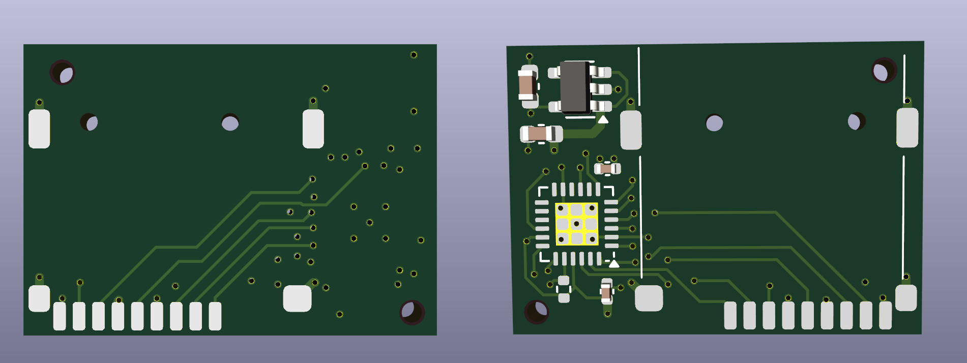
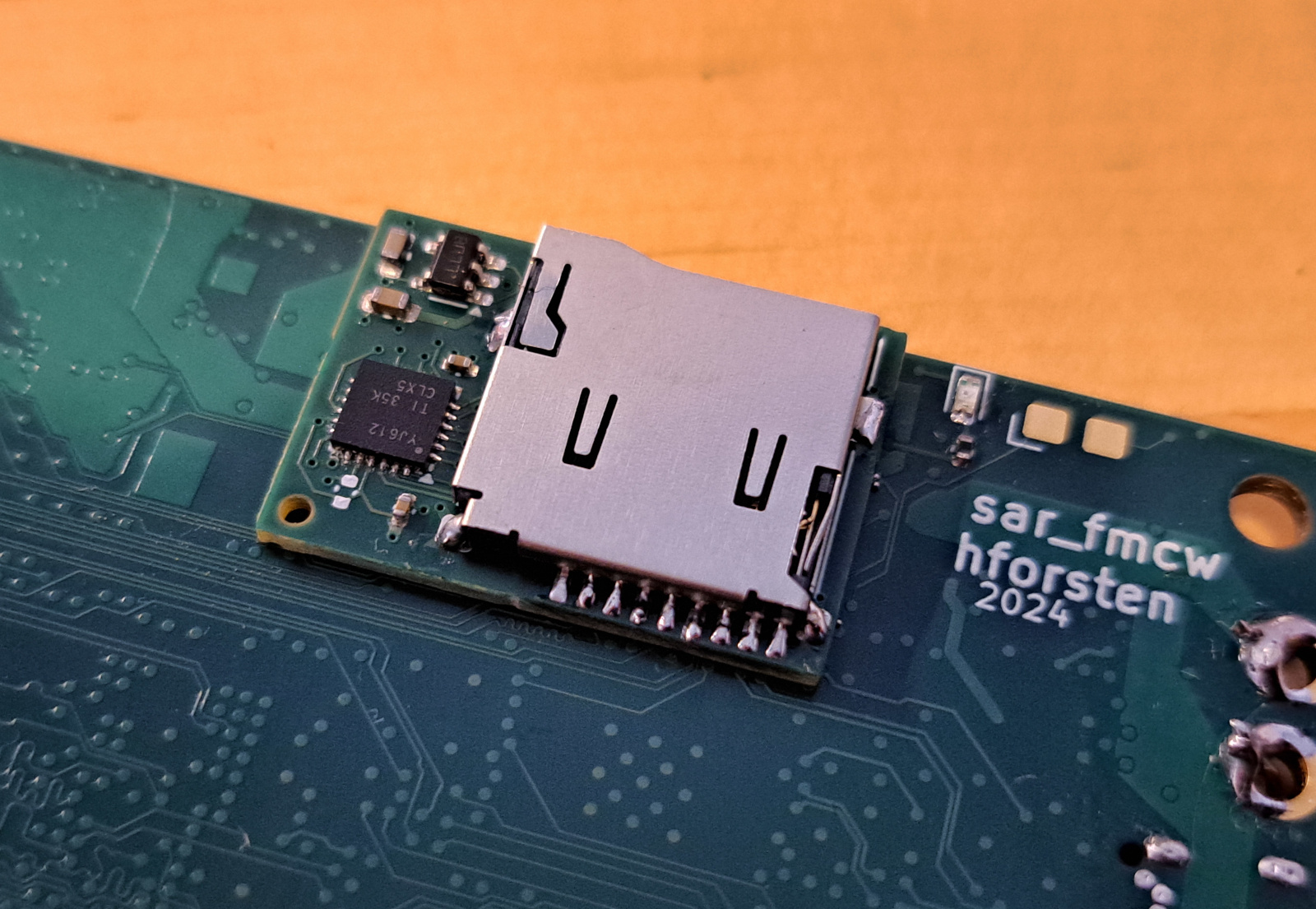
Interposer PCB bottom (left) and top (right).
Above is the PCB I designed. It's a 4 layer PCB with mirrored SD card footprint on the bottom that matches the footprint of the incorrectly wired SD card connector. On the other side is bidirectional 1.8 V to 3.3 V level shifter (TXS02612) and 1.8 V regulator. SD card connector footprints are directly on top of each other to minimize the PCB area.
Manufacturing, assembly, and shipping of 5 copies this PCB cost 43 USD.
Soldering
Solder paste manually applied to the SD card connector pads.
I started with applying some solder paste to the pads on the bigger PCB.
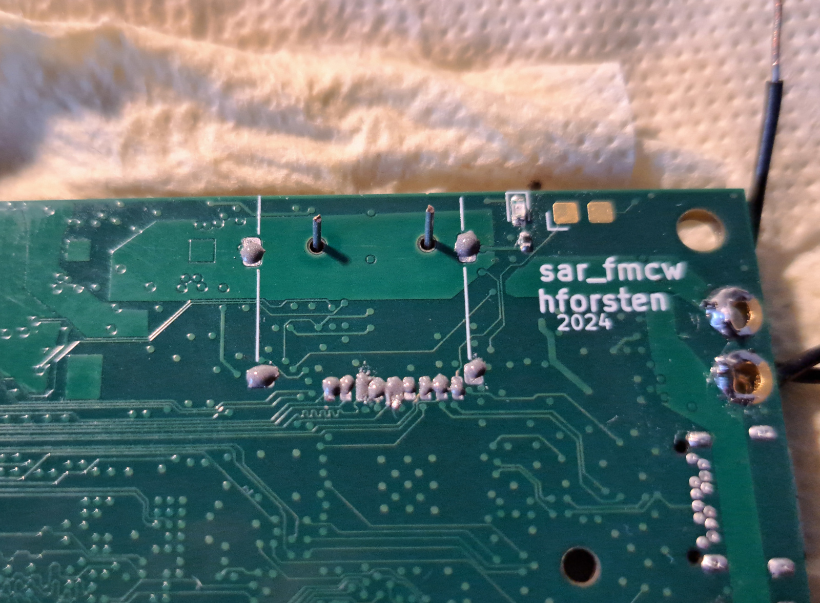
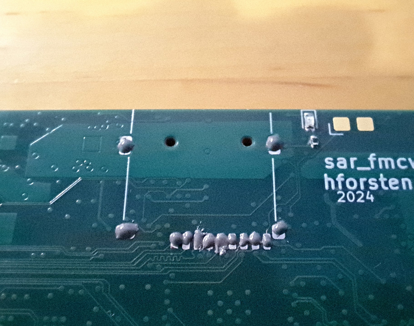
Wires for positioning.
I found it hard to position the interposer PCB correctly because the pads are completely covered by the interposer PCB. Since the SD card footprints were exactly at the same location, the two holes in the footprint also overlapped and could be used to position the interposer PCB. I cut some solid core wire and put them in the holes.
Interposer PCB placed with the guide wires.
Using the solid core wires I was able to position the interposed PCB correctly. This wouldn't have been possible if the SD card connector on the interposer would have been soldered beforehand.
I then heated the interposer with hot air to solder it. It was hard to see when the solder paste had melted since the pads were completely covered by the interposer, but I could see some flux bubbling from under the interposer and the solder joints melting on top of the interposer PCB and I determined it was hot enough. I had placed damp paper towel under the bigger PCB to avoid desoldering components on it which worked fine.
Solder joints seen with a microscope.
Solder joints seem fine when viewed with microscope. Although my microscope's image quality isn't too high, there is no visible short circuits and the contacts seems good.
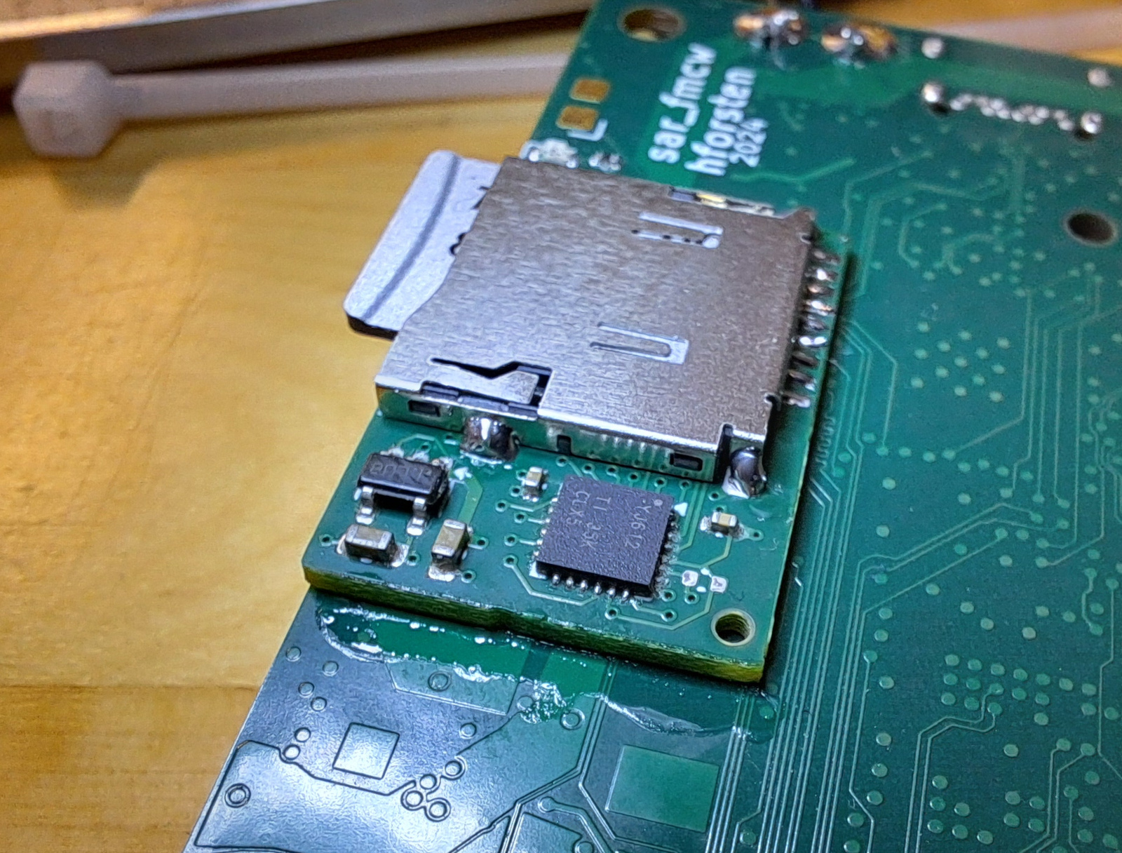
Interposer soldered.
I then soldered the SD card connector on the interposer PCB. It was easy to solder because of the large pads and could be done easily with a soldering iron.
With the added interposer PCB the SD card started to work.
Super glue added.
I added some super glue to the sides for mechanical stability. I didn't think only the solder joints could handle the mechanical stress of inserting and removing the SD card.
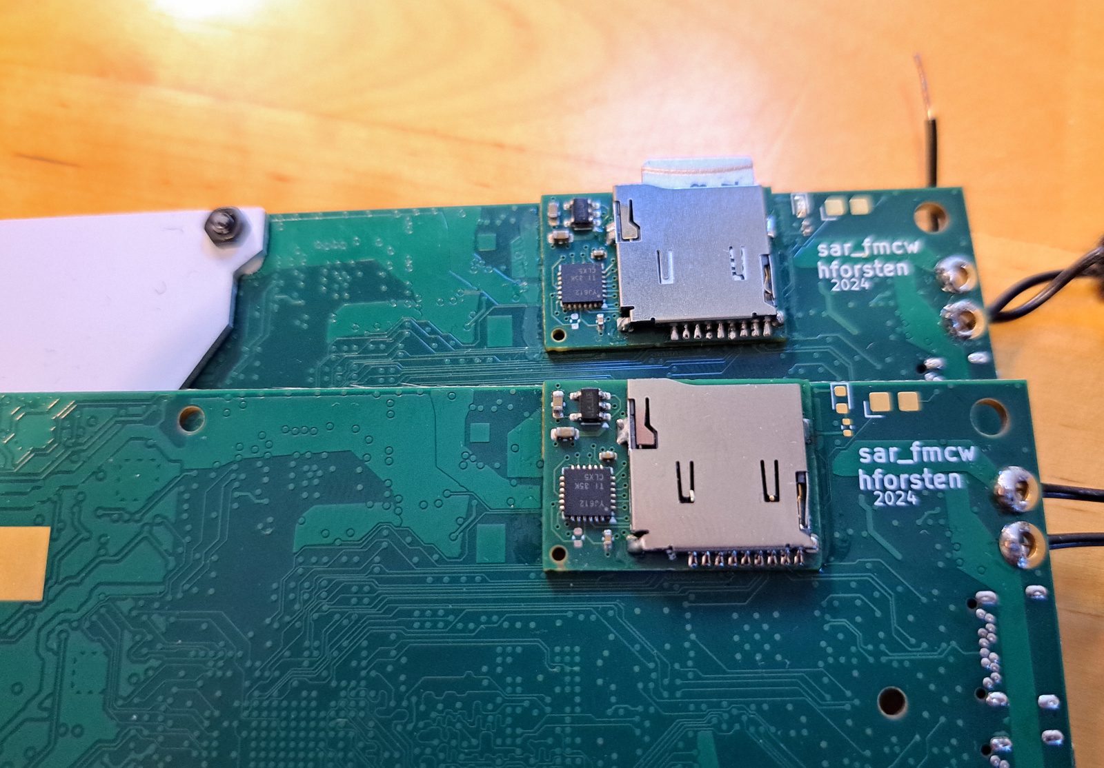
Two fixed PCBs.
I also did the same procedure to another PCB which also worked fine.
Conclusion
Fixing incorrectly wired component can be fixed with interposer PCB if there is enough extra space for the PCB to fit into. Soldering it can be difficult and requires hot air tool. Fixing this PCB with the interposer cost about 50 EUR compared to over 500 EUR for respin of the board.