Introduction
Last year I made a simple vector network analyzer for measuring S-parameters of microwave circuits that I'm making at home. Budget was very small and it was mostly a proof of concept for a low cost homemade VNA.
If you don't know what a vector network analyzer is I recommend that you read the previous post first, but in short it is a test device that can be used to measure magnitude and phase of transmitted and reflected power of a circuit. For example amount of power reflected back from antenna should be low at its working frequency.
While it worked and I could use it to measure one and two-port S-parameters measurement accuracy was not very good. One port measurements worked reasonably well but the biggest problem with two port measurement accuracy was leakage between the test ports. To even calibrate the instrument I had to use an exotic 16-term calibration that can compensate for different leakage paths between the receiver channels.
Lack of isolation between the ports was the biggest issue, but there were also many other smaller issues:
-
Receiver noise figure was very high since there wasn't any amplification before the mixer. Increased noise figure resulted in noisy measurement and reduced dynamic range.
-
Linearity of the receiver was not very good. This was partly caused by the bad choice of IF amplifier and partly because I used a balanced mixer without a balun. Mixer is recommended to be driven with differential input, but wideband baluns were too expensive. Driving the mixer with other input terminated was possible but linearity, conversion gain and noise figure suffered.
-
Directional couplers were integrated on the PCB and to save PCB area I made them as small as possible. At low frequencies coupling was very low and the signal to noise ratio at the receiver was not very good. At high frequencies directivity and matching of the couplers started to worsen.
-
In theory even if the matching, directivity or leakage were high they can be corrected by the calibration. In reality there is some amount of drift and noise in the instrument that causes the vector error correction to not be exact and some amount of error shows up in the results. There was enough drift, non-linearity and noise that there were significant errors in the measurement results even after the calibration.
-
Microcontroller was not fast enough to do any signal processing and all the signal processing needed to be done on the PC. This required transferring raw ADC values through the USB connection to the PC for processing. While the PC should be fast enough to process the samples without delaying the next measurement, in practice my code was written in Python which just wasn't fast enough to do all the signal processing without delaying the measurement. Microcontroller was also busy with reading the ADC and didn't have time to do anything else at the same time.
In total there were enough room for improvement that I wasn't be happy with the board and decided to make an improved version that tried to fix the problem points as well as I could while still keeping to cost low.
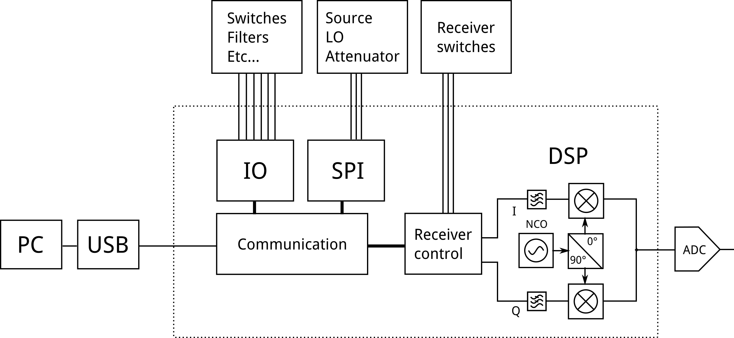
Single receiver VNA
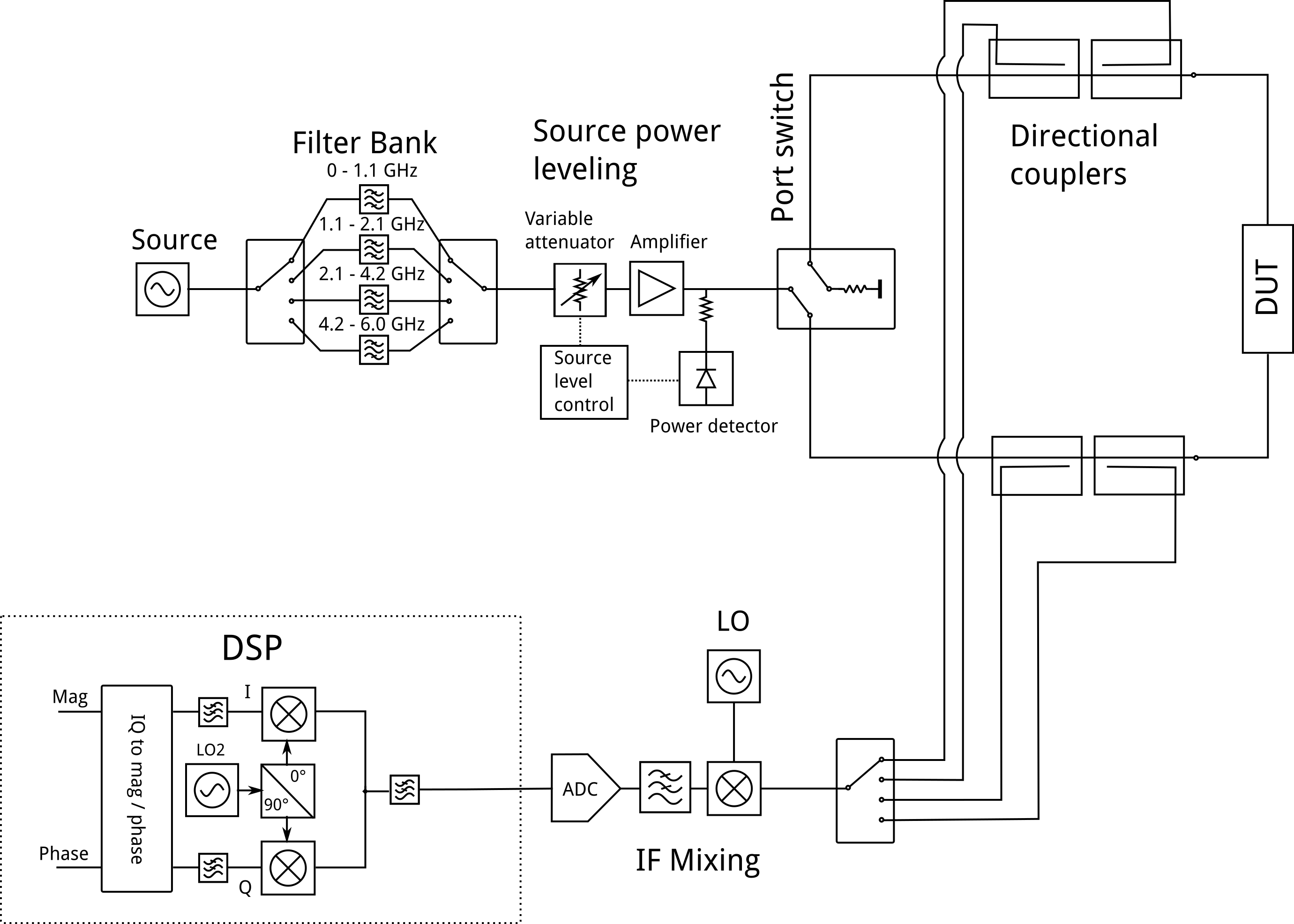
Block diagram of the previous VNA version.
Above is the block diagram of the previous version of VNA. Commercial VNAs use four separate receivers with their own mixers and ADCs to maximize the isolation between the receiver channels and improve the measurements speed. I would also like to use the four receivers, but the reality is that multiplying the receiver cost by four is too much for my budget.
The isolation between the receiver channels can be improved by improving the isolation of the receiver SP4T switch. On my previous VNA I used a single PE42441 SP4T switch. It was very cheap, but the isolation is not good enough for VNA use. Commercial VNAs have isolation at least more than 100 dB between the receivers, but this switch has only 40 dB isolation at 6 GHz.
VNA should much higher isolation than the isolation of the component being tested and for example the isolation of the receiver switch couldn't be measured on the previous version of my VNA since leakage between the receiver channels is the same order as signal passing through the switch being measured. This is a general issue with test equipment: Its performance should be better than device being measured.
In addition to the receiver SP4T switch, port switch also had a single SP2T switch that didn't have good enough isolation. Source switch was PE42423, which is marketed as having an exceptional isolation of 43 dB at 6 GHz. While it is a very good isolation for a single SP2T switch it is not enough for VNA usage.
Achieving a isolation of more than 100 dB on a single PCB is hard and that is why professional RF test equipment have each system shielded from each other. If several blocks are made on the same PCB a milled aluminium case is placed on top of the PCB that isolated the blocks from each other and the environment. Aluminium block can also serve as a heat sink and reduce the temperature drift of the instrument. However I can't afford any custom milled aluminium pieces and have to manage without them.
I did however put a shield around the receiver that can be attached using clips so that it can be removed if needed. Shielding source, switches, couplers, FPGA and power supply would have also been a good choice, but it would have required too much space on the PCB so I decided to leave them out.
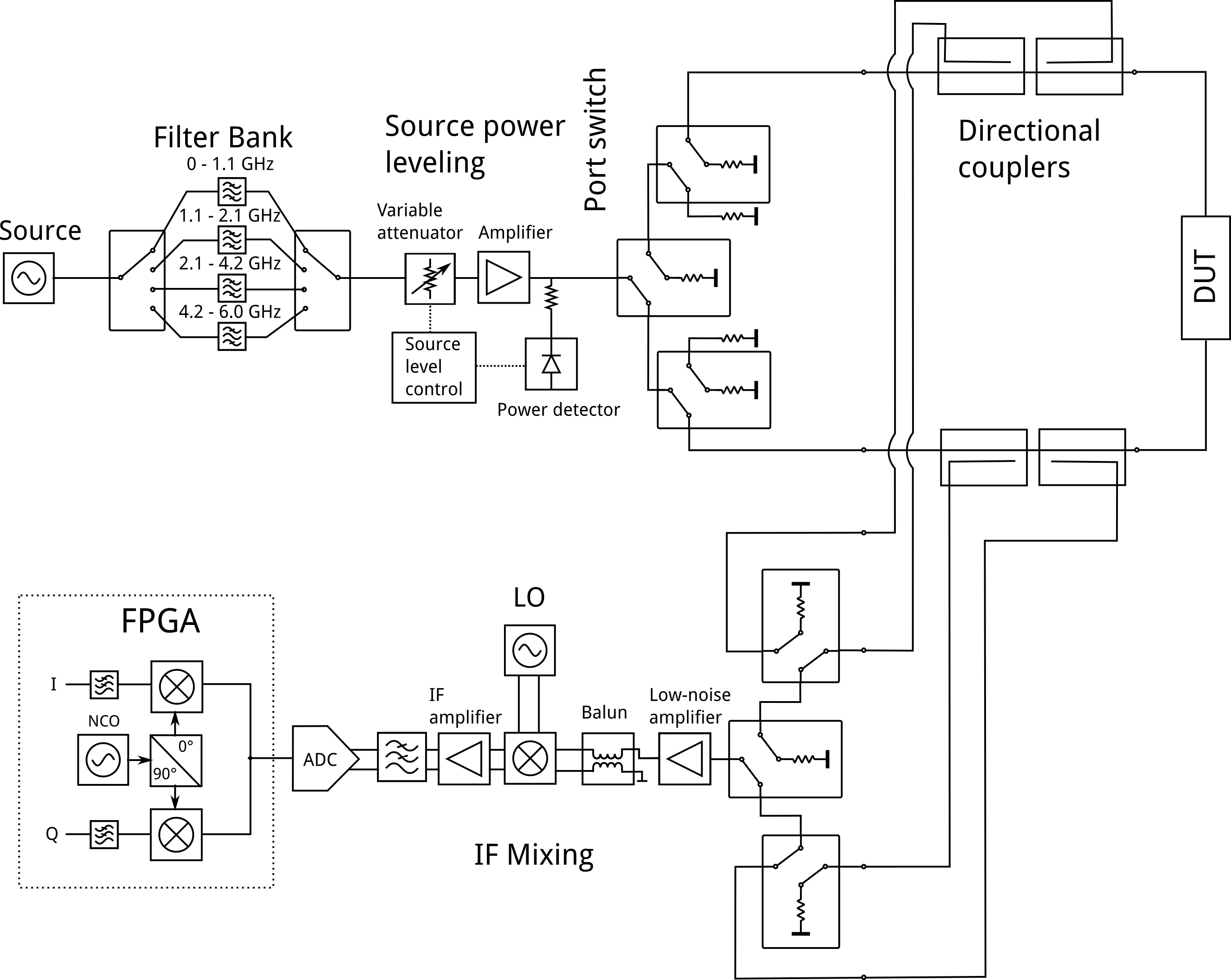
Block diagram of new VNA.
Above is a block diagram of the new VNA design. It is very similar to the block diagram of the previous version presented above. Port and receiver switches are changed to multiple SP2T switches in series as a single switch can't provide the necessary isolation. A low noise amplifier is added before the mixer to reduce the noise figure of the receiver.
Balun is also added before the mixer to increase its performance. Mixer is designed to be used with a balun that converts the single-ended RF signal to differential, but a wideband balun was too expensive. Only Minicircuits sells a wideband enough balun. It costs 8 € a piece with minimum order of 20 pieces plus shipping costs. Ordering the baluns would have cost more than all the other components combined, so I decided to leave it out and accept the performance loss in the first version. However I found a third party seller that sells the same balun for little extra at low quantities. With balun input return loss, conversion gain, noise figure and linearity of the mixer are improved.
Even though the block diagram looks very similar, there are also other big changes:
-
Microcontroller is replaced by FPGA which can do the digital signal processing on the board reducing the computing power required from the PC. On-board processing is much faster and the measurement speed should increase as it isn't necessary to transfer all the ADC samples to PC anymore.
-
ADC was previously a 12-bit ADC integrated on the microcontroller that was sampled at 10 MHz. It is now replaced by a 14-bit external ADC that is sampled at 40 MHz. This should greatly increase the dynamic range of the receiver.
-
Directional couplers were integrated on the PCB in the previous version but now they are on separate PCBs. This allows experimenting with different couplers and improving them without replacing the whole VNA.
-
Receiver is shielded from the other components. To improve the isolation from source to receiver, receiver is heavily isolated from everything else. RF signals are routed on the internal layers of the PCB with top and bottom ground planes to shield the signals as much as possible.
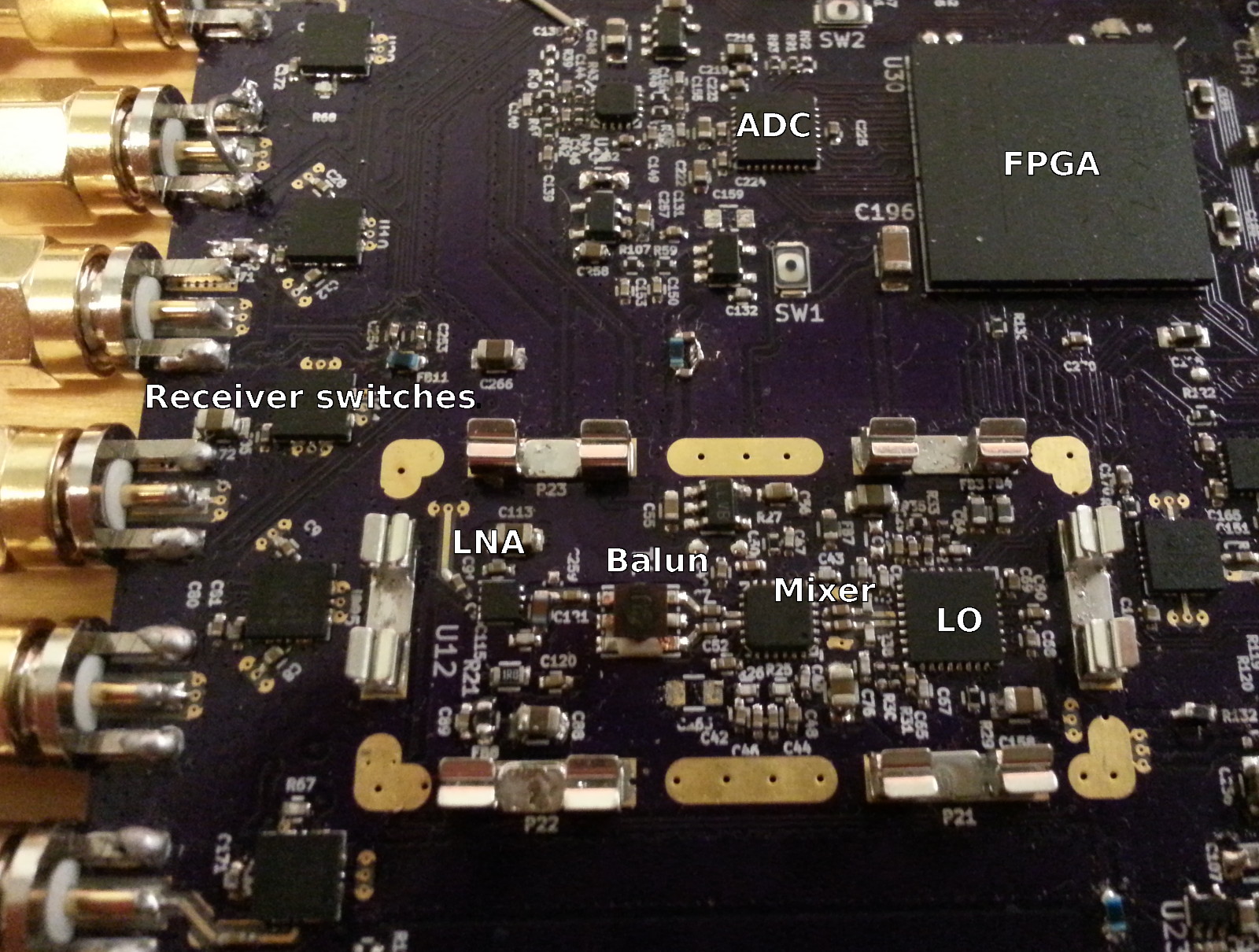
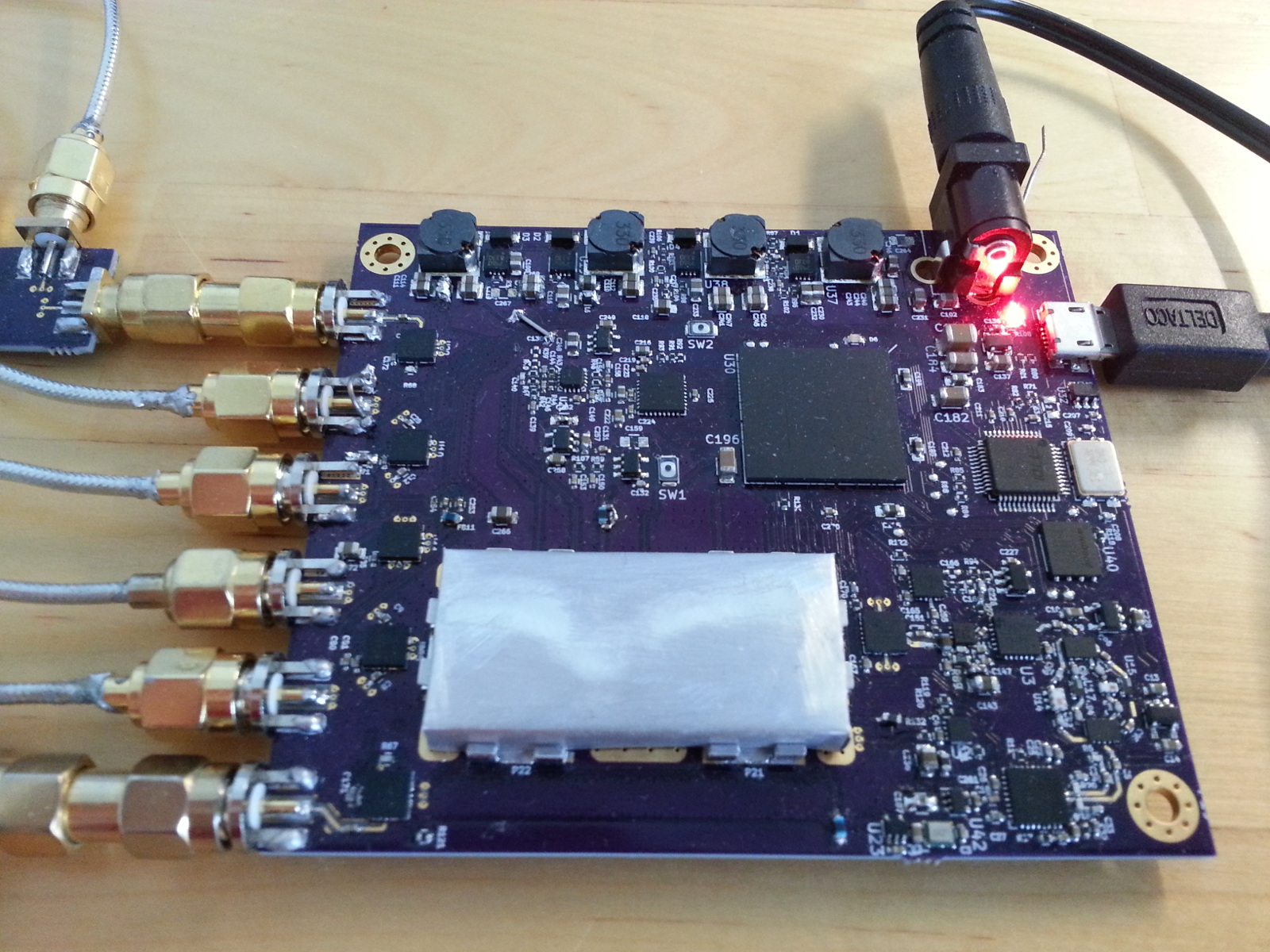
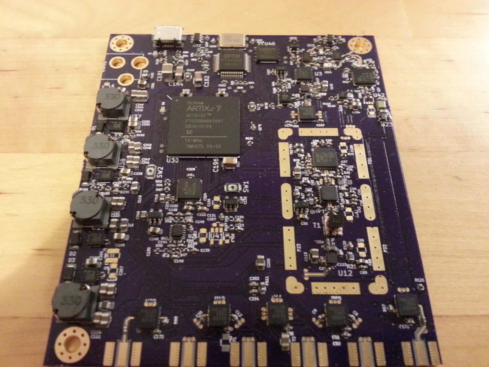
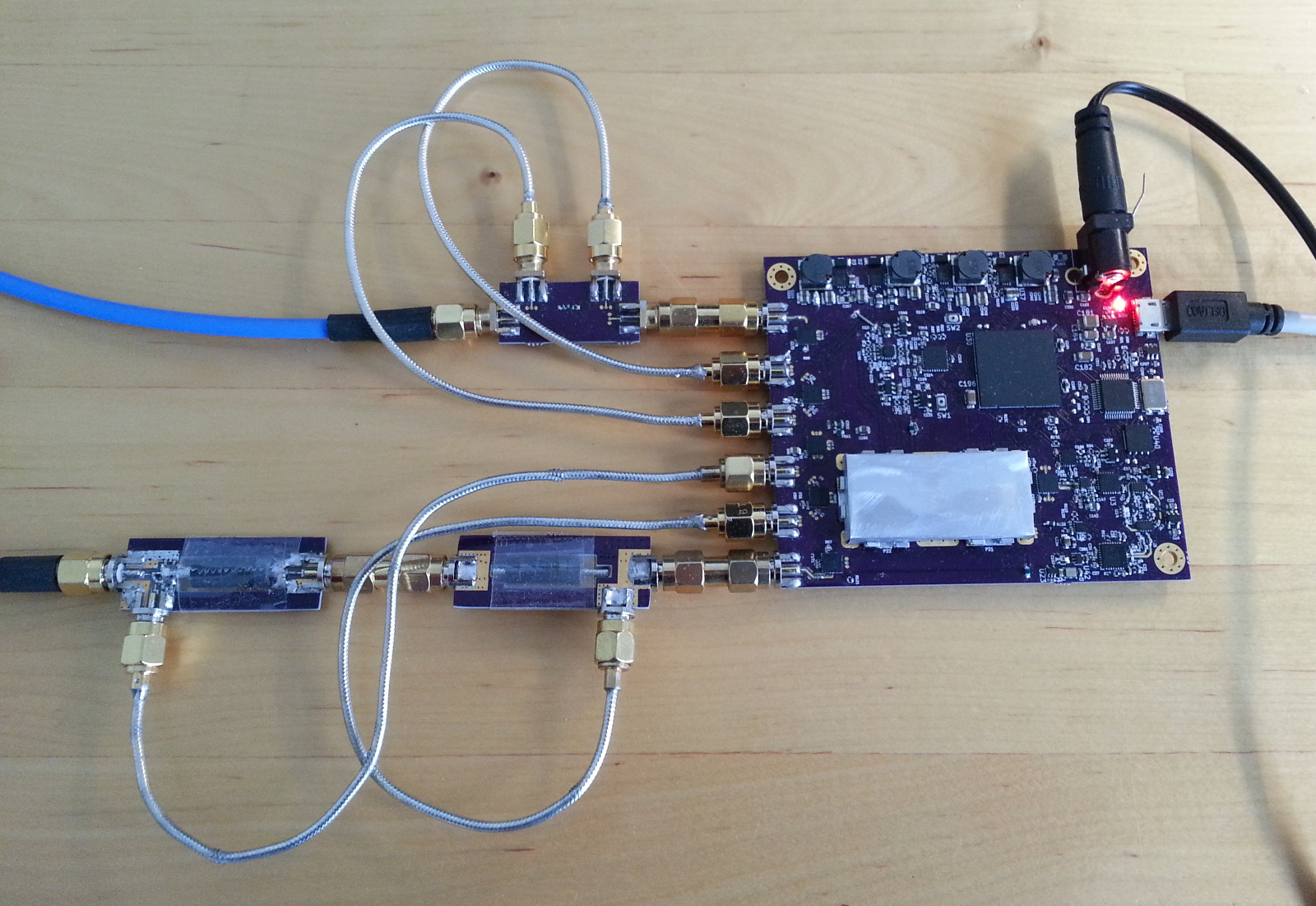
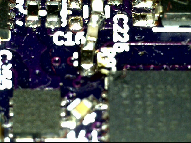
Receiver components labeled.
Above is a picture of the finished receiver section with different components labeled. Shield requires lot of space on the board, but it didn't affect the final PCB size too much, because SMA connectors and power supply limit the minimum board size.
Design
Schematic
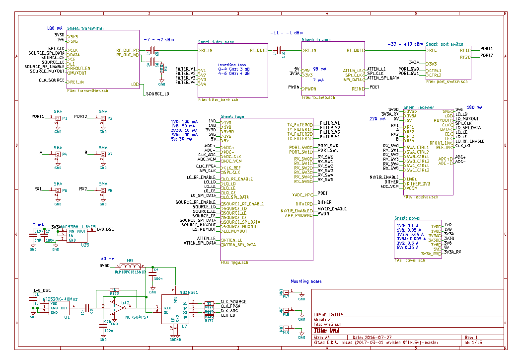
Schematic. Click for PDF.
Mostly due to addition of FPGA number of sheets in the schematic almost doubled from 8 in the first version to 15 in the new version. BOM has 522 components, but it also counts for example mounting holes, RF footprints and test points that are PCB features. There are also many empty footprints that are not meant to be populated just in case. For comparison the previous version had 342 components in the BOM.
FPGA
Simplified FPGA block diagram.
Most of the high level logic, such as calculating the S-parameters from receiver readings and deciding the frequency points in the sweep, are done on the PC. On-board FPGA is responsible for low level processing such as toggling the IO lines based on the commands from the PC and calculating the IQ values from the ADC samples.
Digital signal processing works in the same way as the first version. ADC samples are divided in two branches where they are multiplied by \(\cos(2\pi f t)\) and \(\sin(2\pi f t)\). Frequency of the digital LO is the same as the output of the mixer, 2 MHz in this case. This results in the signal being mixed down to DC. Next average of the samples is taken resulting in two numbers I and Q.
Alternate way of thinking the DSP is that multiplying by sin and cos and then taking averages is equal to one frequency bin of Fourier transform:
This is the optimal way to measure amplitude and phase of a signal with known frequency affected by gaussian noise.
Directional couplers
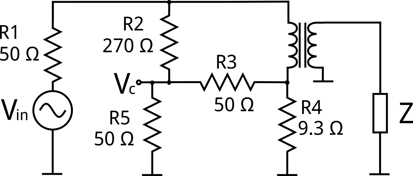
Resistive bridge coupler schematic. R1 and R5 are termination resistances of source and load and are not on the board. Z is the unknown impedance being measured. Vc voltage varies depending on the Z.
The previous directional couplers were stripline coupled line couplers that had two closely placed lines on internal layer of the PCB. It did work quite well at about 2-4 GHz but at lower frequencies the lines were very short compared to the wavelength of the signal and coupling was very low. This caused the receiver input power to be very low at low frequencies leading to very noisy measurements. Above 4 GHz directivity of the couplers wasn't very good. Ideally the coupler measuring the reflected signal wouldn't couple any signal going from the source to the test port and only couple the signals returning from the device under test going towards the source. In practice directional couplers have finite directivity and some of the signal passing from source to DUT is also coupled to the receiver. This directivity error must be measured during the calibration and removed from the measurements. Subtraction of the directivity error isn't perfect and it is preferred if it is low enough so that potential errors between the measured and real directivity doesn't cause big error in the measurement result.
For the new directional couplers I decided to change the architecture to resistive bridge coupler as it can give very flat coupling over very wide bandwidth from kHz frequencies to over 10 GHz. As the name says it is based on resistors that don't have frequency dependence like coupled lines and the frequency response is only limited by parasitics. Commercial VNAs often have resistive bridge couplers to reach the kHz frequencies where transmission line based couplers aren't practical.
A resistive bridge is basically a variation of Wheatstone bridge. A coaxial balun is inserted to the bridge to allow connecting a single ended load. Normally the coaxial cable should be long compared to the signal wavelength, but lower frequency limit of the balun can be extended by adding ferrite beads around the coaxial cable. Ferrite beads attenuate the common mode signals at low frequencies and allow using a much shorted coaxial cable.
Resistor values are also modified a little compared to the normal Wheatstone bridge circuit, so that through loss is lower and coupling loss is higher. See this paper for a good overview on how this coupler architecture works.
Design of my coupler is based on this IEEE paper.
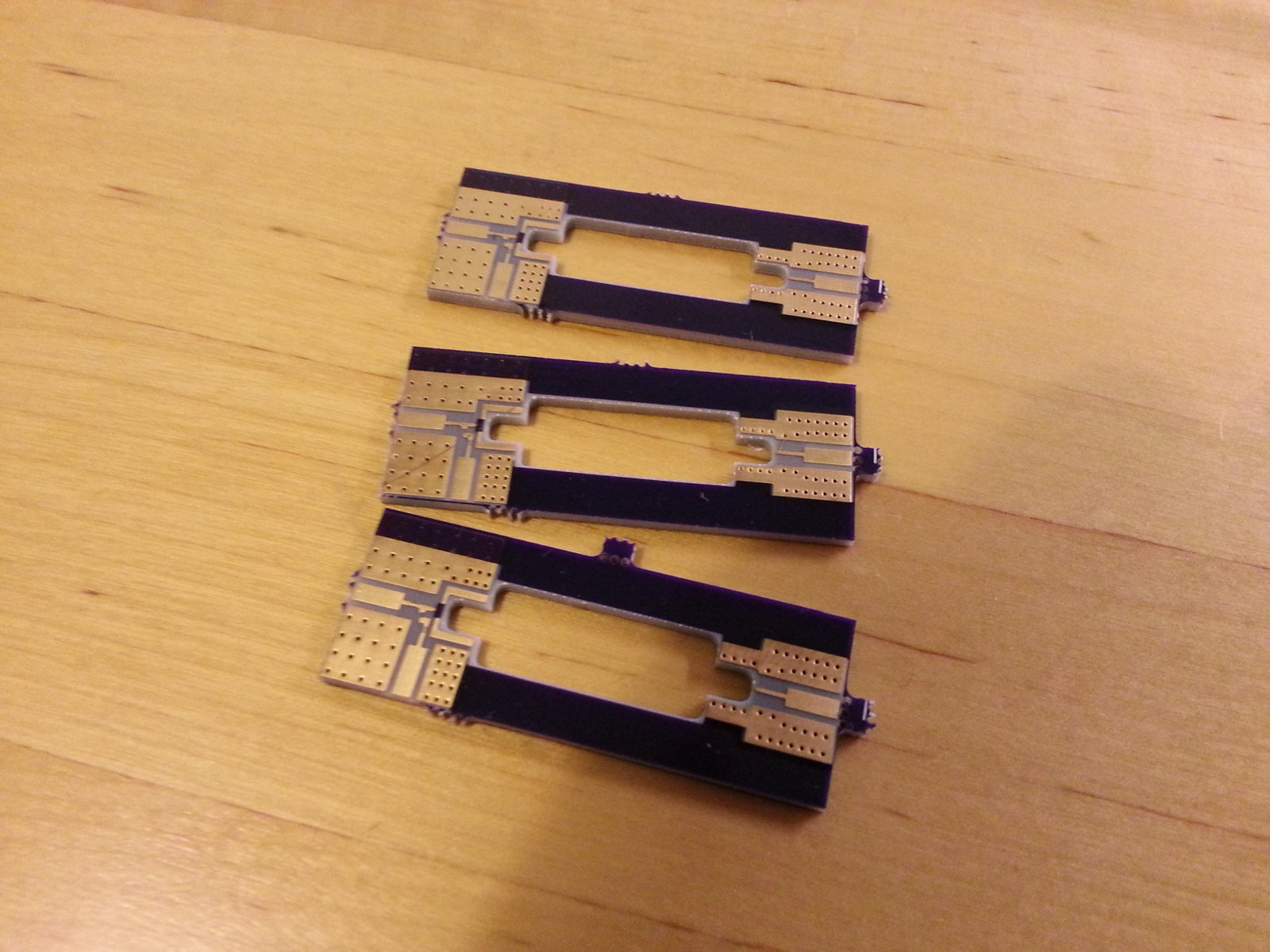
Directional coupler PCBs.
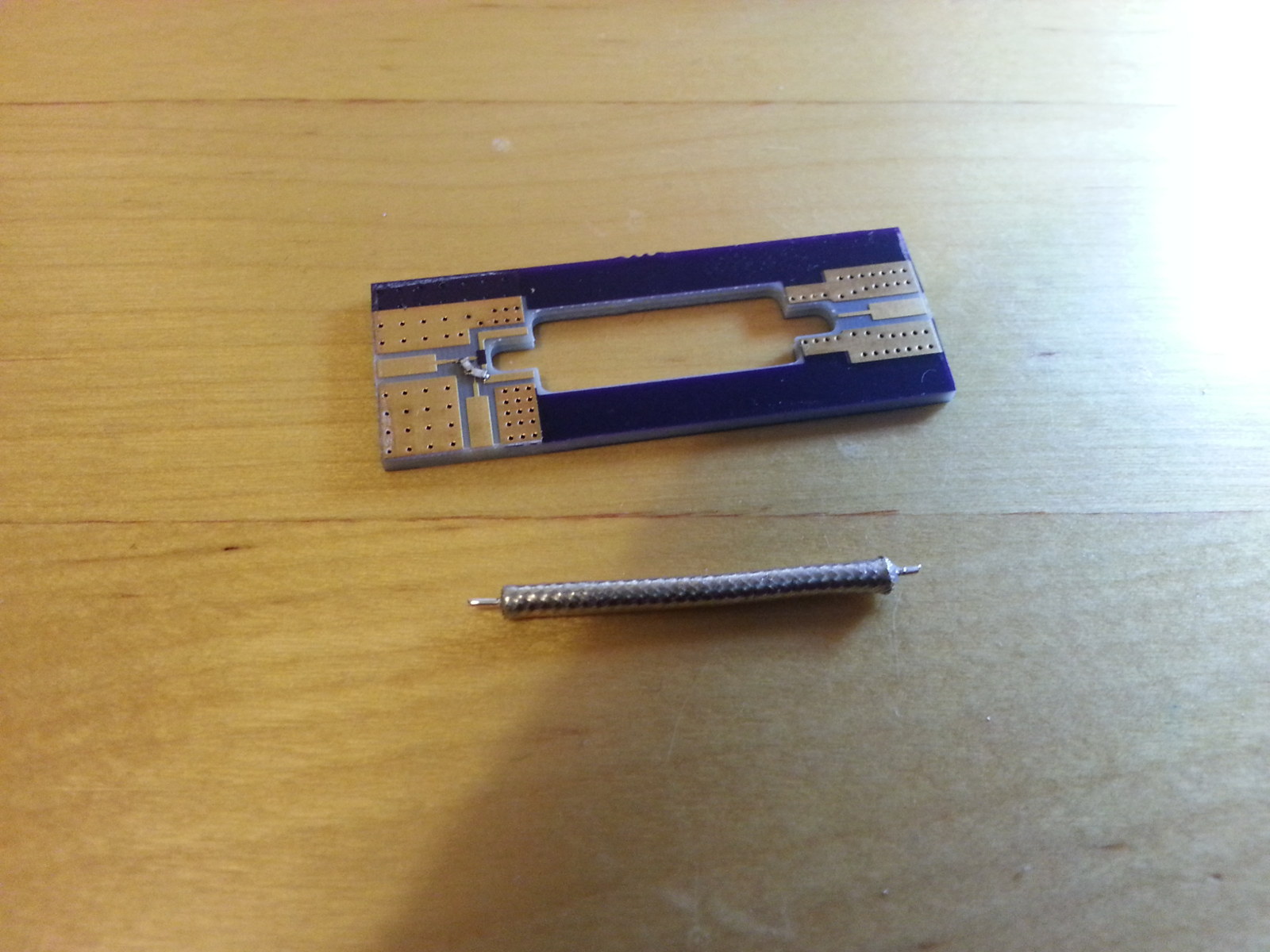
Short piece of coaxial cable for balun.
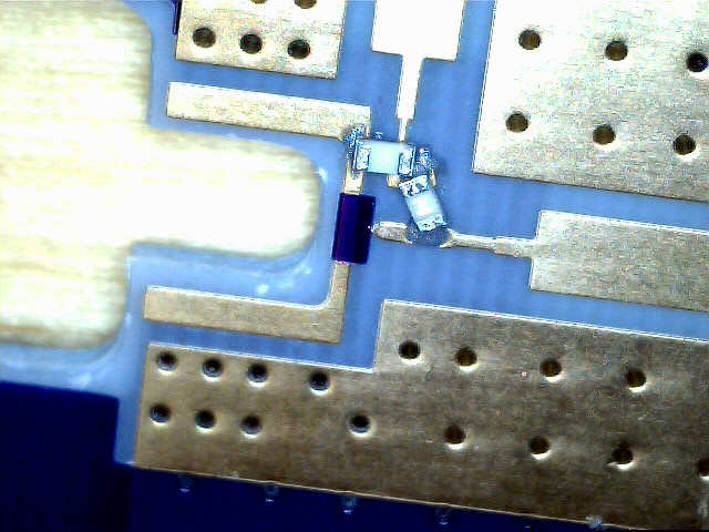
SMD resistors are soldered upside down to minimize parasitics.
At least in theory SMD resistor soldered upside down should have little bit lower parasitic inductance than when it's soldered the right way. The resistive element is on top side of the resistor and by mounting it upside down it is closer to the PCB ground plane lowering its inductance.
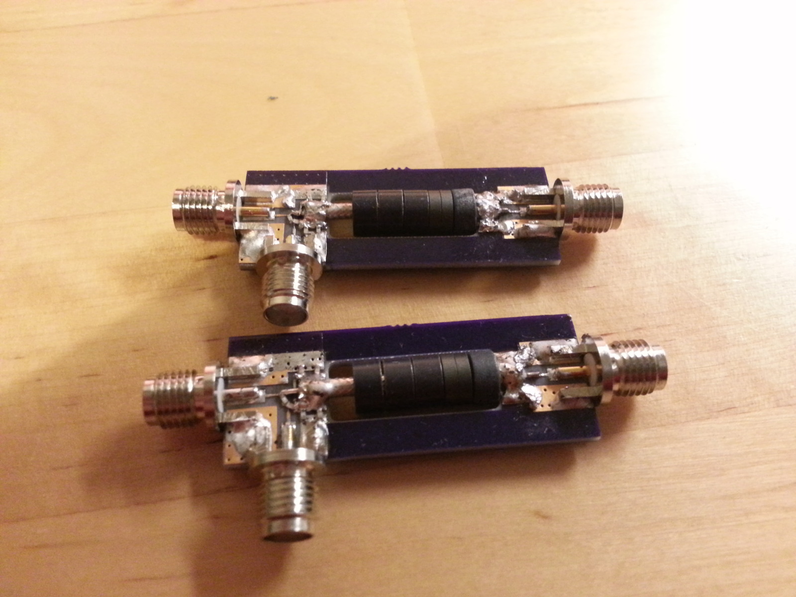
Two finished couplers with ferrite beads around the coaxial cable.
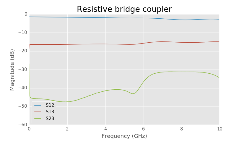
Measured S-parameters of the coupler.
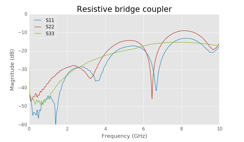
Measured S-parameters of the coupler.
In the above plots are measured S-parameters with a commercial VNA up to 10 GHz. Coupler was measured as a two port with third port terminated with a high quality termination from the VNA calibration kit.
S12 trace is the through path, S13 is the coupled path and S23 is the isolated direction. Directivity is S13 - S23 and it is better than 25 dB up to 5.5 GHz and about 15 dB after it. Matching is very good at low frequencies but starts to worsen as the frequency increases. Through loss is about 1.5 dB.
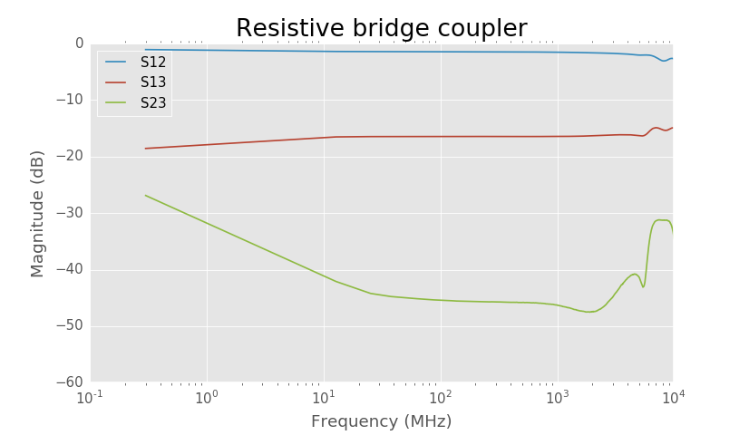
Measured S-parameters of the coupler. Logarithmic scale.
Low frequency performance can be more easily seen when the X-axis is changed to logarithmic. Ferrites on the coaxial balun extend the low frequency range and the coupler still has about 5 dB directivity at 300 kHz.
Overall I'm very happy with the performance of the coupler. Matching, directivity and flatness of the coupling are all much better than the coupled line coupler on the previous version of the VNA. Using these couplers should result in much more accurate measurements.
Soldering
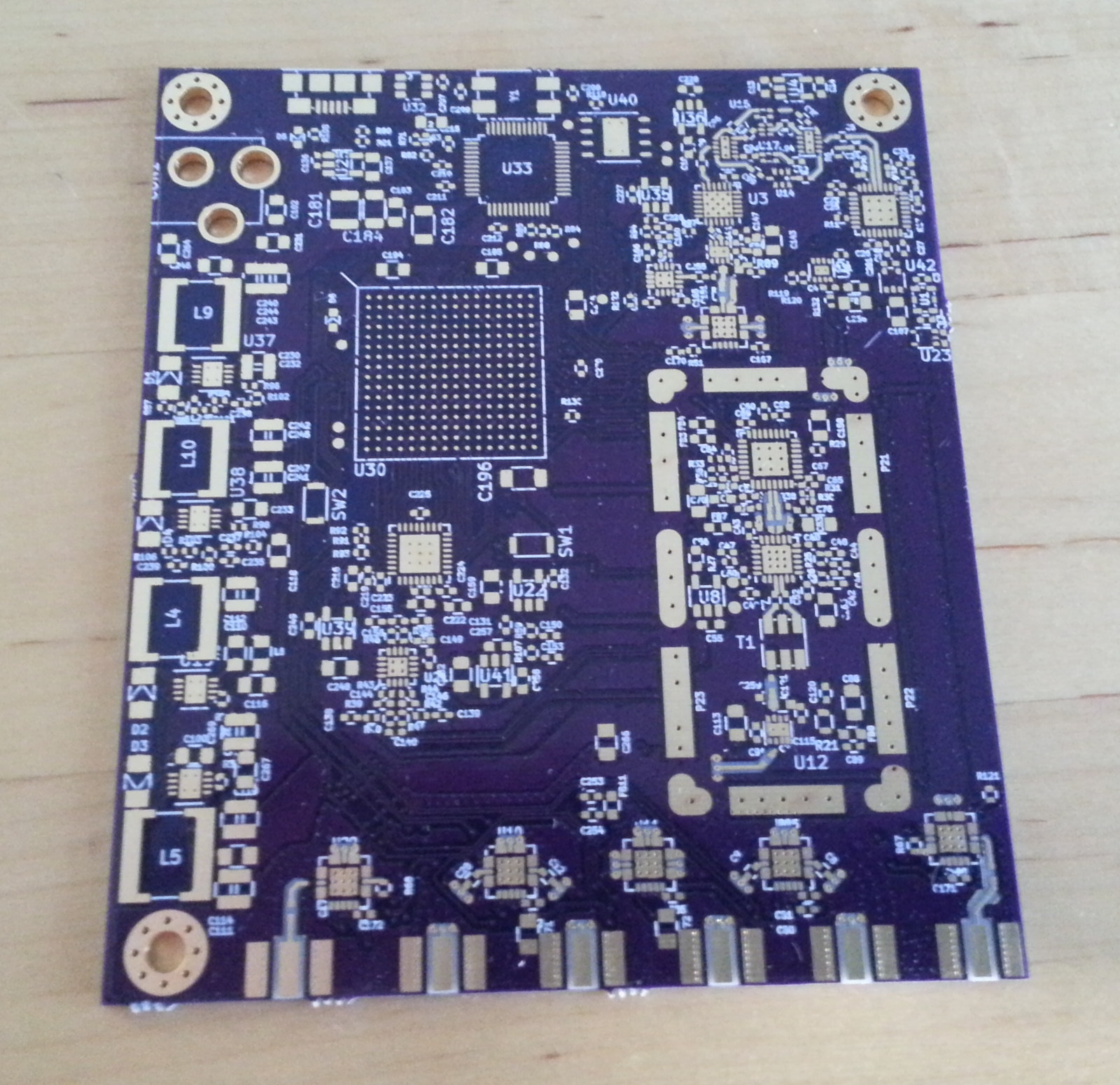
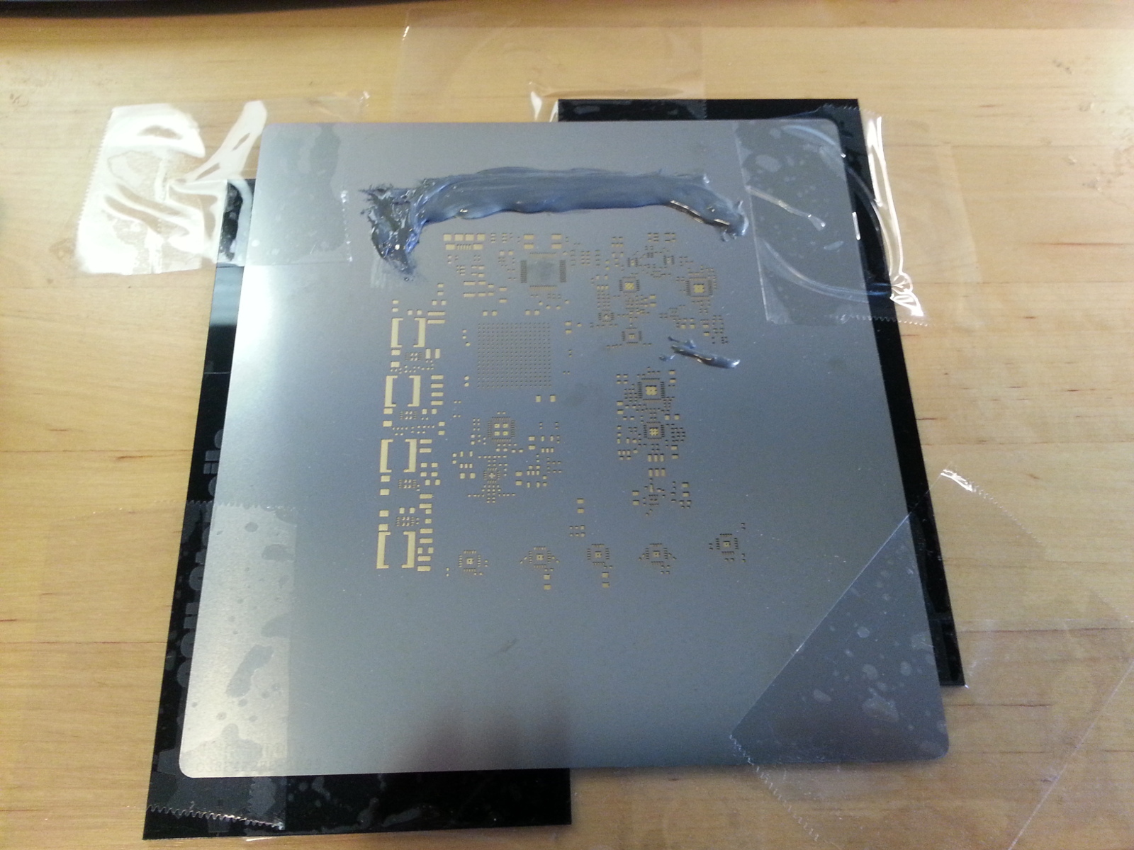
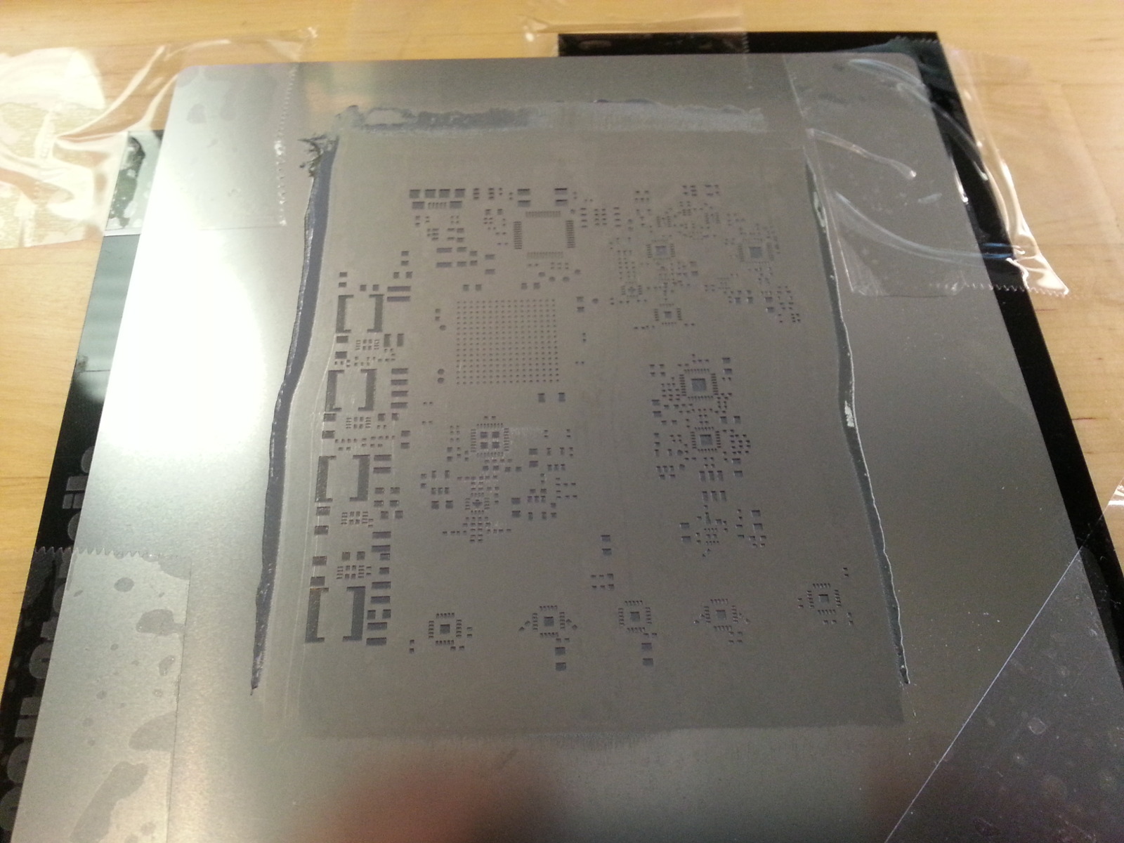
Bare PCB.
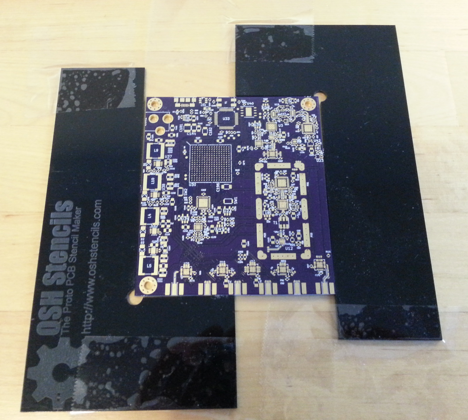
PCB secured for solder paste stenciling.
Like the first version, PCB is from OSH Park. OSH Park offers 4-layer FR408 substrate PCB that has lower loss and better controlled dielectric constant at high frequencies. It seems to currently be the only cheap non-FR4 process and if you have read my other posts I have used it a lot.
Previously I have made the backside of the PCB first, but I have found that it makes applying the solder paste on the front side more difficult as the board won't sit straight on the table. This time I decided to do the front side with difficult components first and do the backside by hand later. Having a flat backside without components helped with securing the PCB and the stenciling result was better than the last time. Stainless steel stencil should also help with the solder paste application and should result in better defined edges of the deposits than polyimide stencils I have used before. Stencil is from OSH stencils.
Solder paste on stencil.
After spreading the paste.

Solder paste on BGA footprint.
Solder paste on RF source components.
Solder paste stenciling was very successful. Edges of the paste deposits are very well defined.
BGA placed on the solder paste. Ball pitch is 1 mm, which is very easy to position even by hand.
Xilinx FPGA comes in a 256 ball package with 1 mm ball pitch. It is very big pitch for a BGA package and makes it very easy to solder at home. There is also comfortable amount of room to route all the signals even on a low cost PCB like this.
Components placed on the paste.
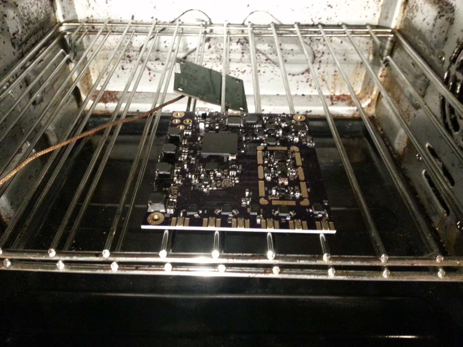
PCB in the reflow oven.
I used the same old toaster oven for reflow that I have made all my other projects with. Green PCB on the back holds the temperature sensor.
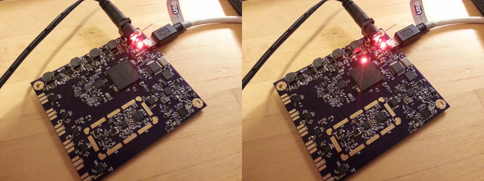
Hello world!
I made a quick bitfile for FPGA that just blinks the LED and everything worked the first time.
Measurements
Receiver
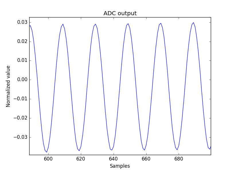
ADC output waveform.
External 14-bit ADC makes a big difference to the receiver dynamic range compared to the previous 12-bit ADC integrated in the microcontroller. Mixer output frequency is programmable and is set to 2 MHz in the above plot. Exact frequency isn't important, but there are some limits for setting the frequency. At low frequencies there is a dithering signal and more noise and at high frequencies linearity of the IF amplifier and ADC isn't as good. At some point the anti-aliasing filter will also start to attenuate the signal. 2 MHz is a good compromise.
Sampling frequency of the ADC is 40 MHz. In theory it could be much lower without aliasing and high sample rate ADC costs more so why not use for example 10 MHz ADC instead? There are three reasons:
-
To simplify the clock distribution FPGA, PLLs and ADC use the same clock signal. 40 MHz is a good value for all of them. If different clock frequencies were used, clock dividers or PLLs would be need to be added. FPGA could use separate clock, but PLL reference clock and ADC sampling clock need to be synchronized.
-
High sampling speed allows using simpler anti-aliasing filter.
-
Sampling speed can be traded for accuracy. When two consecutive ADC samples are averaged dynamic range increases by 3 dB. Quadrupling the sampling speed and taking average of four samples increases dynamic range by 6 dB, which equals increase of one bit in the sample depth. Dynamic range of 40 MHz 14-bit ADC is equivalent to 10 MHz 15-bit ADC or 2.5 MHz 16-bit ADC.
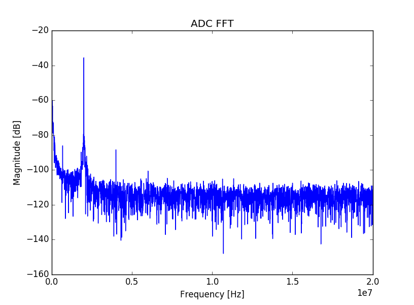
FFT of 5000 ADC samples. Y-axis is dB full scale. Maximum non-clipping input sine wave would be 0 dB.
Above is an FFT of 5000 ADC samples which is the maximum I can store at the FPGA and transfer to the PC at the moment. USB is not fast enough to continuously stream the ADC samples. Noise floor is about -105 dBFs. 5000 samples corresponds to 8 kHz wide FFT bin and sampling time of 125 µs. Every doubling of the sampling time increases the dynamic range by 3 dB. With 10 ms sampling time (100 Hz IF bandwidth) dynamic range is 125 dB and 0.1 s (10 Hz IF bandwidth) gives a dynamic range of 135 dB.
For comparison the previous version had dynamic range of 90 dB with sampling time of 400us. Due to needing to transfer all the samples to PC this setting was about as fast 5 ms sampling time on the new version. Because of better ADC, receiver LNA and on-board processing the dynamic range increased by at least 30 dB for the same measurement speed.
One port S-parameters
Making accurate one port S-parameter measurements is much easier than two port measurements. Error model is much simpler and isolation isn't as big of a problem. One port measurement can be completely corrected with three parameter error network, while two port error network has at least nine parameters.
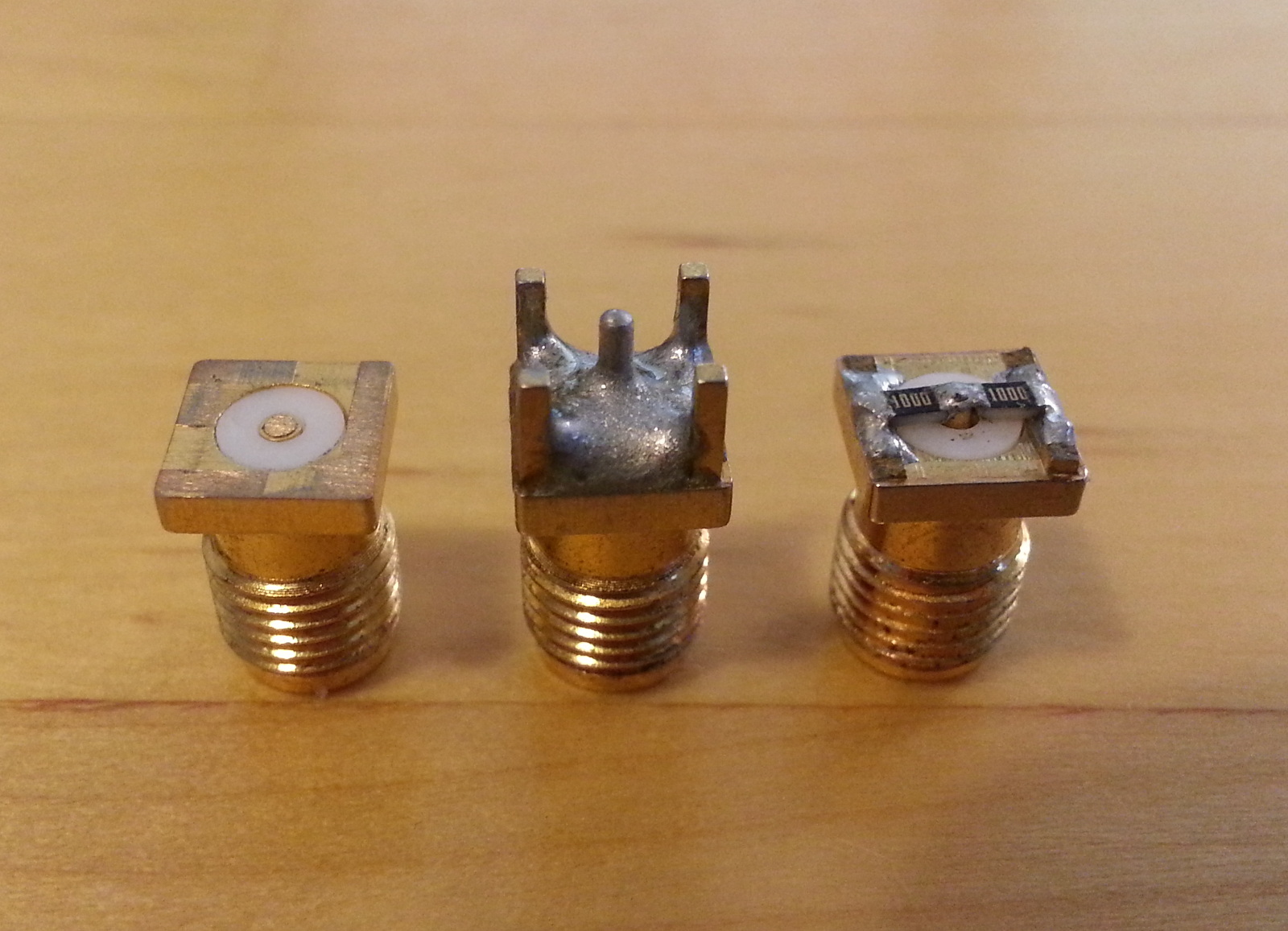
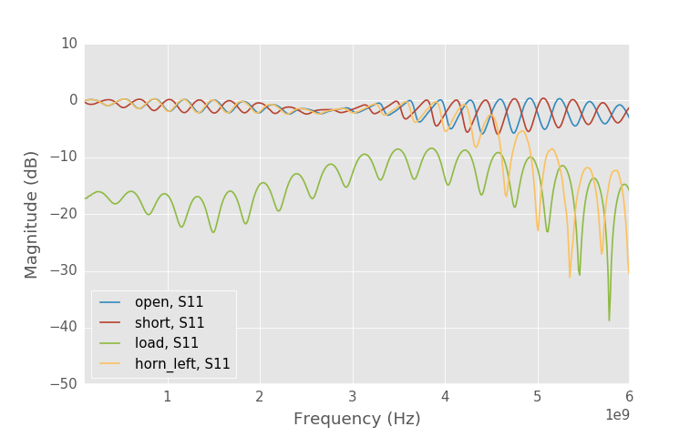
Homemade SMA calibration kit. Open, short and load.
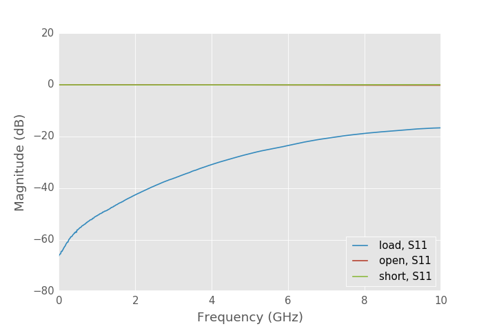
Measured calibration kit S-parameters.
Previously I didn't have information about the true S-parameters of the calibration kit and had to make a guess that decreased the accuracy of the measured S-parameters.
I measured the S-parameters of the calibration kit with commercial VNA calibrated with a very accurate and expensive calibration kit. This basically transfers the calibration of the expensive kit to my homemade kit and allows me to make reasonable accurate measurements with the homemade kit.
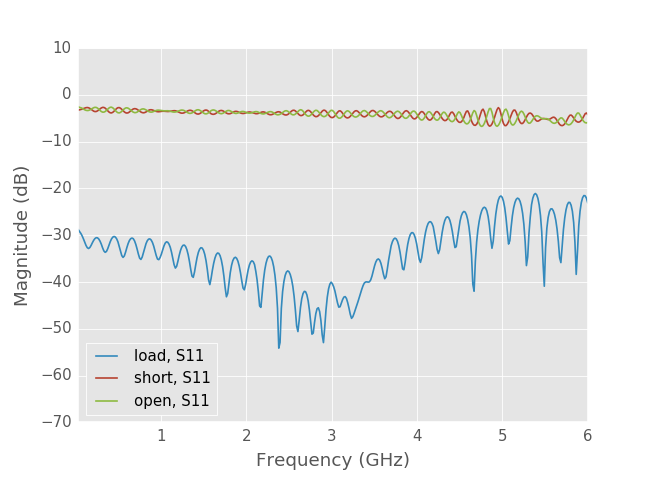
Uncalibrated S-parameters of the calibration standards.
Above are the raw uncalibrated measurements of the calibration standards measured with my VNA. Load is measured to be -30 dB because of the limited directivity of the couplers. Ripple is caused by the variation in the source matching. Open and short are not centered at 0 dB, because of loss of the couplers. All these errors can be determined from the measurements and corrected.
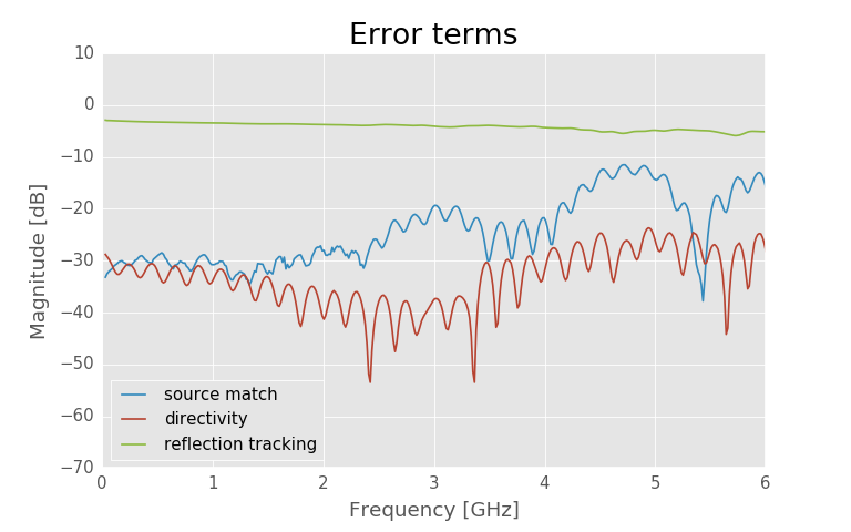
Solved error terms.
Compared to the same measurement with the previous version error terms are now clearly much smaller. New couplers have better directivity and matching reducing the ripple in open and short measurements and improving the dynamic range of the load measurement.
Patch antenna
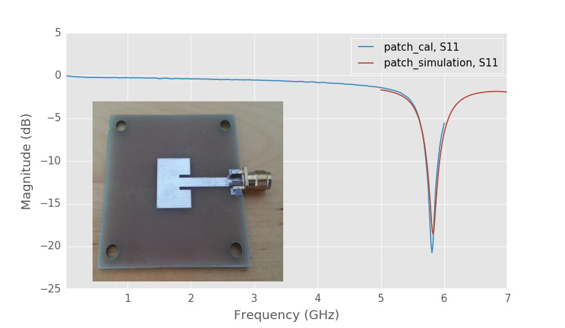
Picture of the patch antenna and simulated and measured S11 traces.
Above is a simple patch antenna designed to work at 5.8 GHz. "patch_cal" trace is the measured S11 and "patch_simulation" is the S11 from EM-simulator. Measured S11 agrees very well with the simulated one and the trace is very clean.
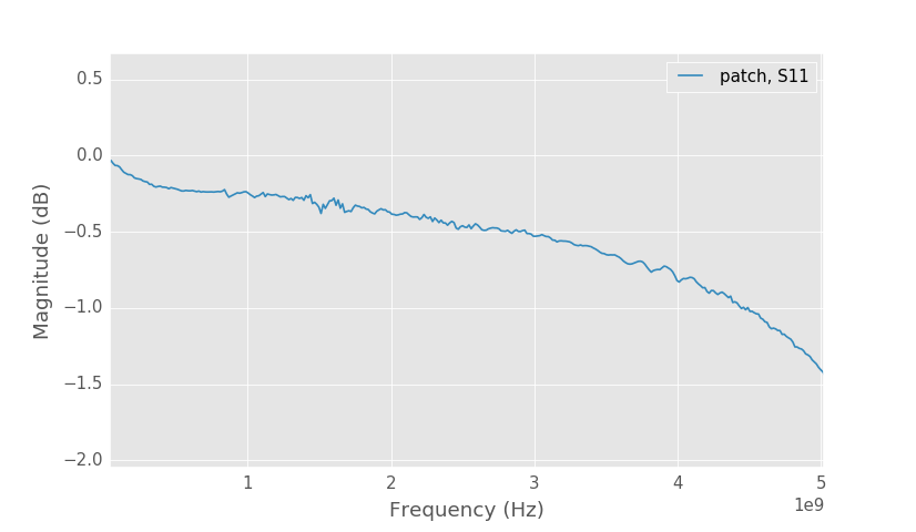
Zoom into patch antenna S11 trace.
Trace noise in the patch antenna S11 measurement is about 0.1 dB, which is probably caused by the variation of the leakage from source to receivers. Below 700 MHz performance is much better because isolation is much higher at low frequencies.
Horn antenna
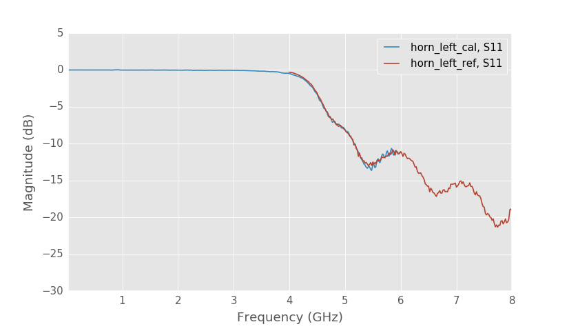
6 GHz radar horn antenna compared to commercial VNA measurement.
Above is a S11 measurement ("horn_left_cal" trace) of my homemade horn antennas compared to a measurement made with a commercial VNA ("horn_left_ref" trace). Compared to the measurement with last version traces are now much closer. Most of the improvement is from measuring the calibration kit.
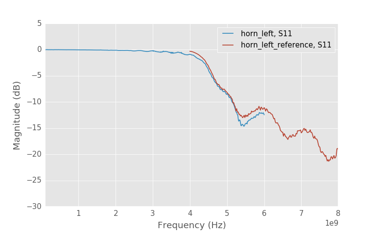
Other horn antenna.
The other horn antenna also agrees quite well.
Two port S-parameters
Resistive bridge couplers on port 1 (down). Stripline coupled line coupler on port 2 (up).
I didn't have enough of the new resistive bridge couplers for both ports. So for two port measurements I had to put coupled line coupler from the previous version on the second port. It reduces the accuracy, but at least it allows me to make measurements.
Previous version had such high leakage between the channels that I had to use a special 16-term calibration that also calibrates for all the possible leakage paths. This version has better isolation and I'm able to use the normal SOLT calibration with isolation calibration (Both ports terminated).
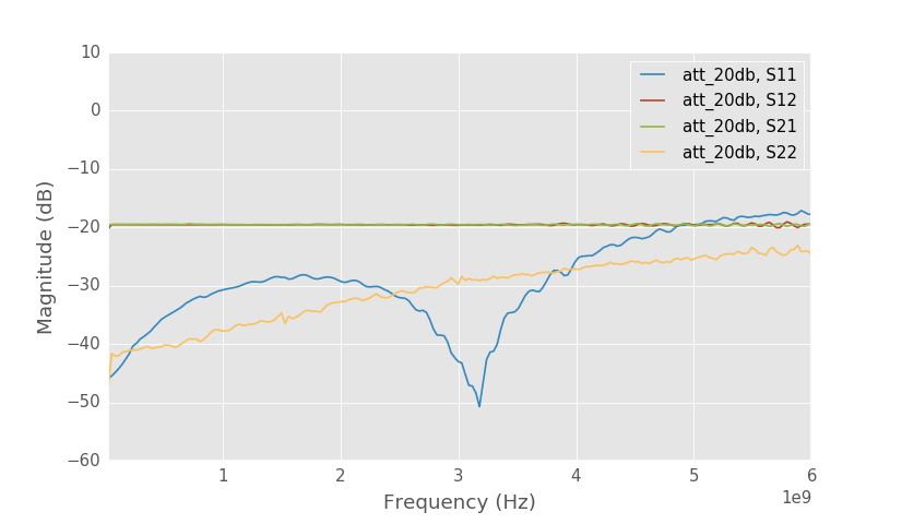
20 dB attenuator S-parameters.
Above are the measured S-parameters of 20 dB attenuator. I measured the same attenuator also with the old VNA and using the same 12-term calibration quality was pretty terrible. With 16-term calibration that includes additional leakage paths I managed to measure it. There's a clear difference in the S11 and S22 accuracy between the new and the old versions. Ripple in the traces is unphysical and they should be smooth.
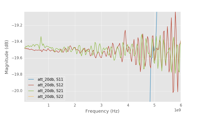
20 dB attenuator S-parameters. S21, S12 detail.
Above is the same measurement zoomed to the S12 and S21 traces. Ripple increases as the frequency increases due to the leakage being bigger at high frequencies. At low frequencies there's also some difference between the S21 and S12 traces due to different couplers on different ports. Port 1 had the new resistive bridge couplers while port 2 had coupled line coupler that has very low coupling at low frequencies which decreases the measurement accuracy.
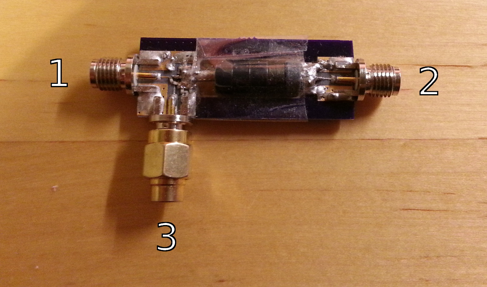
Resistive bridge coupler with ports labeled. Port 3 is terminated with load.
I made three bridge couplers, two are used on the port 1 so one is left to be measured. Above is a picture of the coupler with ports labeled. In the picture port 3 is terminated with load so that it can be measured with two port VNA. Port 1 to port 2 is the through path with low loss. Port 1 to port 3 is coupling path that has 16 dB loss. Port 2 to port 3 is the isolated path with low coupling.
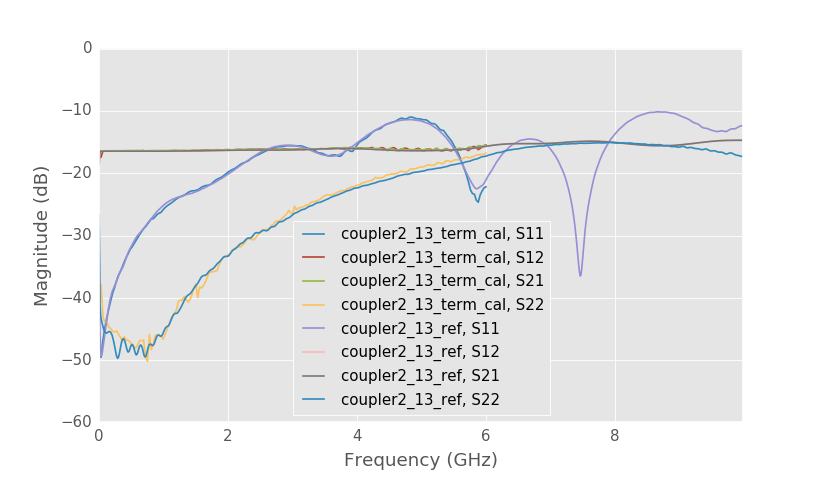
Coupler port 1 to port 3, with port 2 terminated.
In the above picture are the two port S-parameters of the coupler measured with my 300 € VNA calibrated with 5 € homemade calibration kit ("coupler2_13_term_cal" traces) and with commercial 100 000€ VNA calibrated with 5 000€ calibration kit ("coupler2_13_ref" traces). While my measurements are much noisier the traces agree very closely.
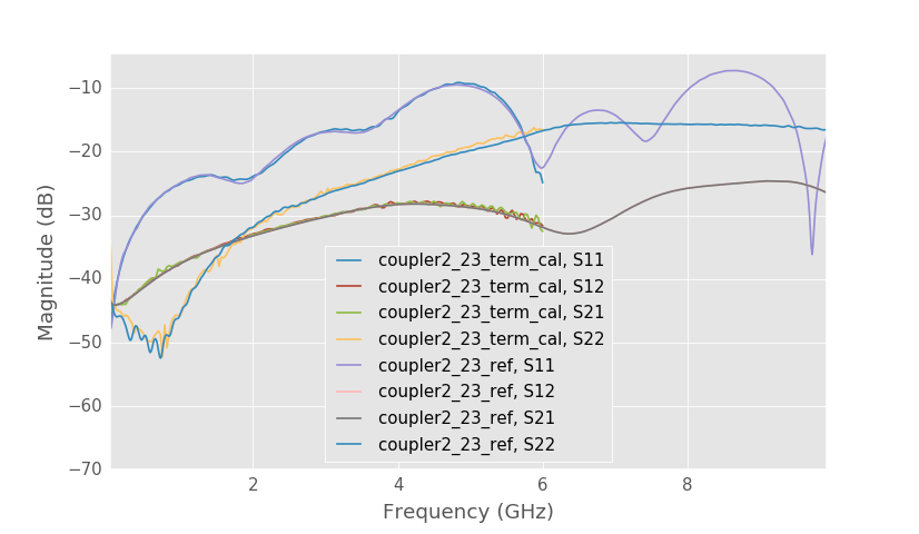
Coupler port 2 to port 3, with port 1 terminated.
Port 2 to port 3 measurement also agrees well. If you compare these measurements to one presented before, you notice that the directivity is not as good. Reason is that these measurements have been made with very cheap termination that has higher reflection coefficient. In the directivity measurement the terminated port reflects some power and measured S21 is bigger than it would be with a perfect termination.
Isolation
Isolation performance of the VNA didn't turn out to be as good as I hoped. I knew before that I wouldn't get the best performance without very good shielding, but I wanted to avoid it as good shielding is too expensive. It seems that most of the leakage is radiative leakage from source to receiver, but there is also more leakage between the receiver channels than expected. I did try to find and fix some of the worst unintentional antennas.
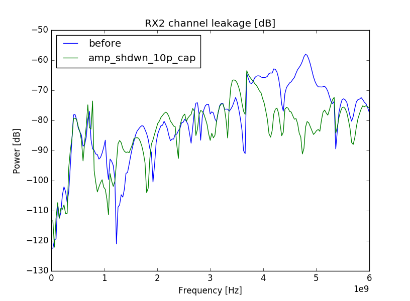
Port 2 reference channel (RX2) measured with source on port 1. With and without 10 pF capacitor on amplifier shutdown trace.
Source amplifier has a shutdown pin that is connected to FPGA and routed on top layer of the PCB for a long distance. I placed a 100 ohm resistor near the amplifier pin to add some loss to the line. However it turns out that at about 5 GHz the shutdown pin trace is the biggest leakage source. After adding a 10 pF capacitor from the trace to ground leakage dropped by 20 dB at 5 GHz.
Amplifier shutdown trace, series resistor and the added capacitor. Skinny trace on the right is the shutdown trace. Source amplifier is the IC on bottom left.
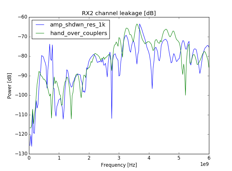
Port 2 reference channel (RX2) measured with source on port 1. With and without hand over the coupler cables.
At about 700 MHz there is another peak in the leakage plot. This one seems to be caused by the external couplers. If I place my hand over both of the couplers leakage is attenuated by about 20 dB.
There are many more similar unintentional antennas and I can't fix all of them. I guess the only way to improve the isolation is to shield every subsystem and preferably even make them on different PCBs.
Stability
On the above video you can see how waving my hand over the board affects the receiver readings. Source frequency is 6 GHz and it is connected to port 1 causing the high readings on the port 1 channels RX1 and A. Test cables are open so ideally RX2 and B channels shouldn't have any power entering them. However due to leakage some power is detected at RX2 and B channels. Moving my hand either raises or lowers the detected leakage based on whether the reflected signal from my hand is in or out of phase with the other leakage paths.
S11 measurement is also affected by the isolation. The absolute effect is smaller because signals are bigger, but I can affect the S11 readings by about 0.01 dB from about 0.5 m away by moving my hand over the VNA. IF bandwidth was 100 Hz.
Trace noise is also visible in the plot at the beginning. It is about 0.002 dB which is quite good but due to the poor isolation trace noise in the measurements is much higher. With a good isolation trace noise would be about this level also on the measured S-parameters.
Conclusion
The new version of the VNA is much more accurate than the previous version. Receiver is very accurate and has good dynamic range, but like the last version isolation limits the performance. A metal case around the PCB would help with stability and should increase the measurement accuracy. With case, shields around the individual subcircuits and receiver on a separate PCB measurement accuracy should be much better.
All the design files are available at Github.