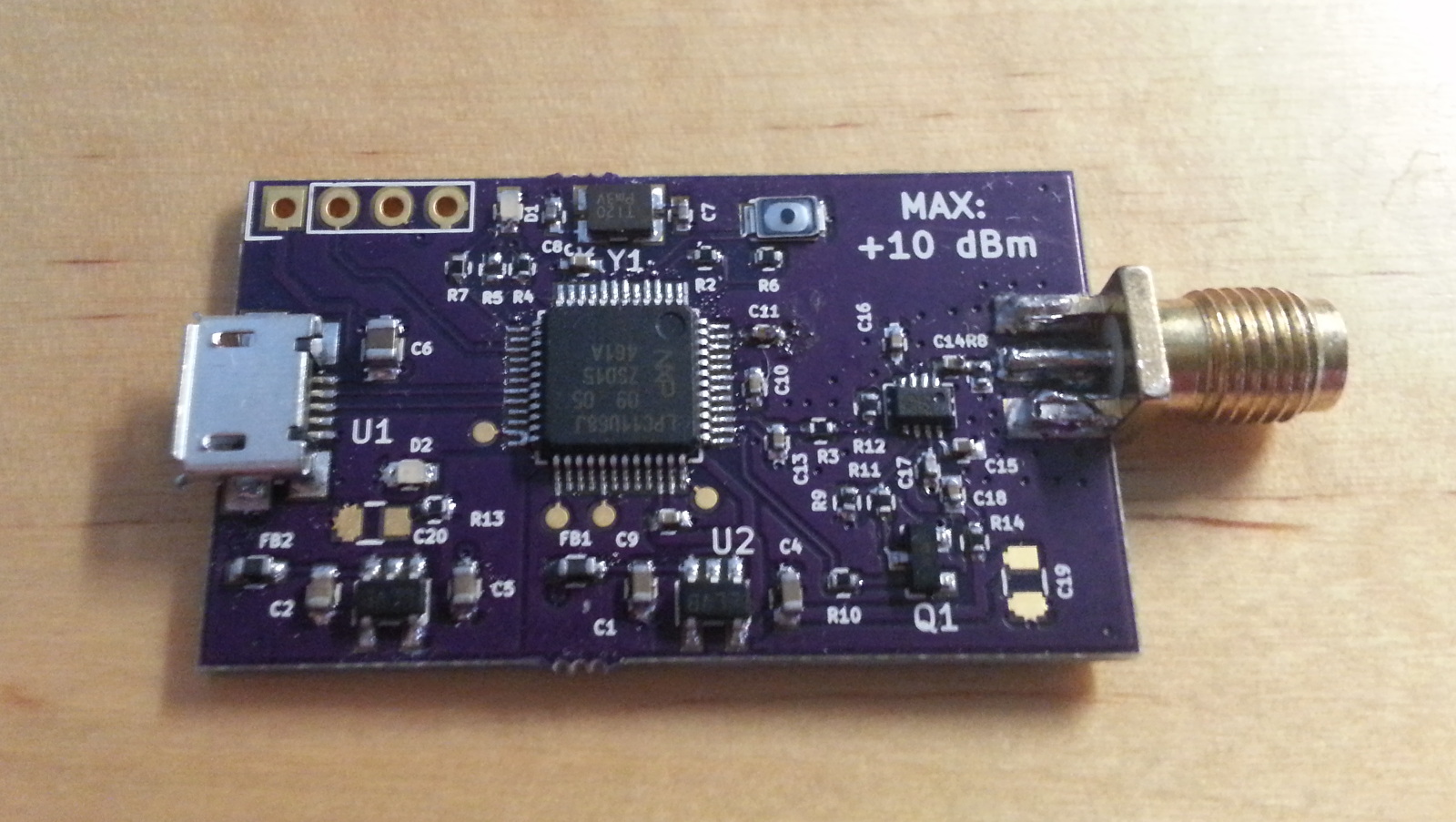
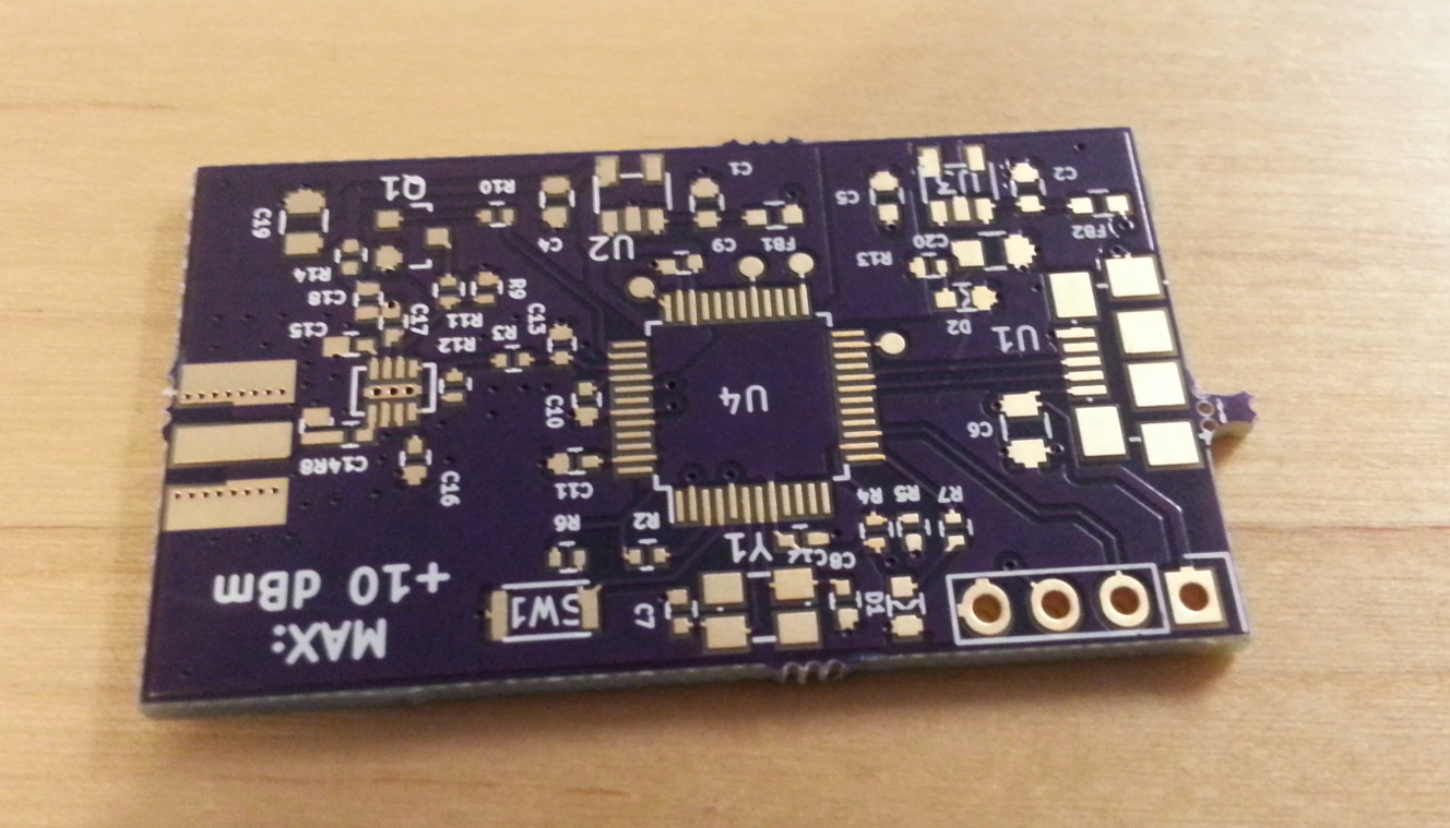
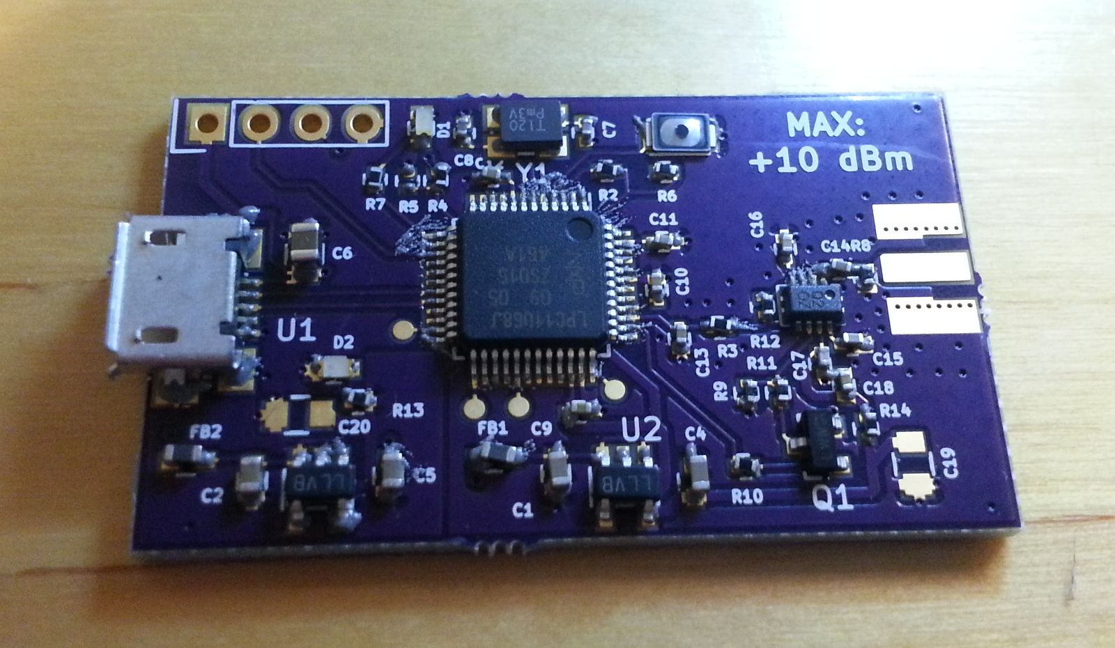
Finisihed power detector.
Introduction
Continuing with the self-made RF test equipment theme I decided to next make an RF power meter. Accuracy of the finished power detector should be good enough for calibrating the output power of my VNA and measuring the output power of my radars. I'll be happy with +- 1 dB accuracy and sometimes even a worse accuracy is useful in measuring if there is any signal at all. USB connection is nice to have so that I can connect the meter to computer and for example automatically measure power of the VNA over the whole frequency range without having to manually write down all the measurement results.
Schematic
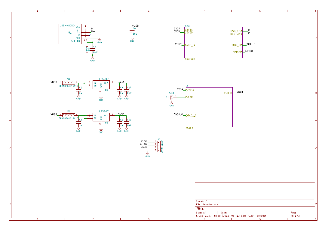
Power detector could be done simply with a diode followed by capacitor similar to peak detector circuit used at lower frequencies. Diode will rectify the RF signal and generates a DC voltage which is proportional to the RF power.
While it would be possible to design the detector using a discrete diode and matching circuit, it is much cheaper, easier and accurate to use integrated circuit already containing the necessary circuit, matching circuit and temperature compensation. Existing ICs are also very well characterized so hopefully I don't need to calibrate the power sensor myself.
Searching on Digikey brings up several power detector ICs with most suitable looking to be AD8319. It works from 1 MHz to 10 GHz, has good accuracy, dynamic range and temperature stability. Package is 8-pin SMD package that can fit on a 2 layer PCB. Using 2 layer PCB instead of 4 would halve the price of the PCB.
I chose to use LPC11U68 microcontroller to interface to the computer. It is very cheap, has USB, doesn't need external programmer and I'm already familiar with some of the other LPC family processors so the programming should be easy. It is available in 48-pin QFP package which also can be routed on 2 layer PCB.
Only a voltage regulator IC is needed to complete the design. Having had a good experience using LP5907 regulator in my VNA I decided to use the same regulator on this project. It has very good power supply rejection ratio and low noise for the price.
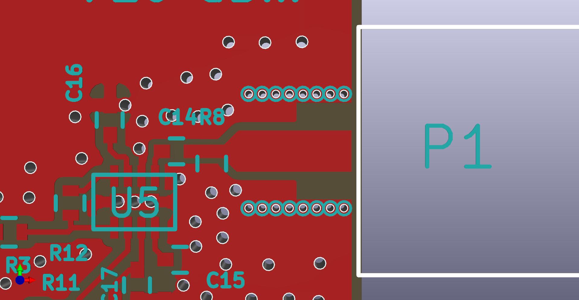
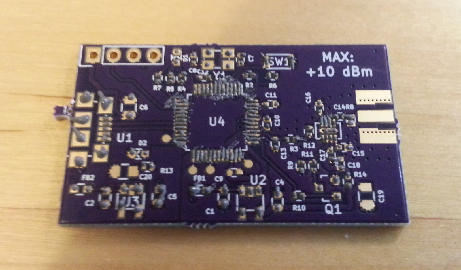
RF traces on PCB. SMA connector on right, matching components and input to power detector IC.
On a 4 layer board SMA connector needed a cutout under the signal pad because 50 ohm microstrip line is only 0.34 mm wide, while signal pad is 1.5 mm. Without the cutout, pad would work as very low impedance transmission line causing reflections. Cutout removes the closest ground under the pad raising its impedance. 2 layer board is so thick that the 50 ohm microstrip is about 3 mm thick and instead ground plane on the top side needs to be brought closer to the signal pad to decrease the impedance of the line.
3 mm microstrip line would be very wide and make it hard to interface with components. Changing microstrip to grounded CPW with 0.2mm ground gap can be used to reduce the line width to 1.5 mm. While it's still quite wide, it's easier to interface with components than 3 mm line.
Manufacturing
Bare PCB from OSH Park.
Manually dispensed solder paste on PCB.
Components added on top of solder paste.
I didn't feel like I needed a stencil on this simple board, so I dispensed the solder paste manually. I did have few short circuits on the microcontroller pins that I fixed manually, but otherwise it worked fine. Soldering was done on my reflow oven made from toaster oven.
Measurements
I don't have a reference power detector to measure the absolute accuracy of the detected power, but I can use my VNA to generate a low frequency signal and measure its voltage with oscilloscope and power with power detector. Power of the signal can be calculated from the oscilloscope voltage measurement and it should be more accurate than the power detector reading. Power detector reading can then be adjusted so that it shows the same power. This method only corrects the reading at one frequency, but datasheet of the power detector has calibration curves that show how the power changes as function of frequency. There's still issue with frequency dependent losses on the PCB, but those can be assumed to be small. As a result power detector should be sort of accurate.
Power detector has limited range of powers that it can measure accurately. I can use my VNA to also measure the linearity range of the power detector. VNA has PE43711 0 - 31.25 dB variable attenuator that controls the output signal power. Attenuator is much more linear than the power detector, so measuring the output power of the VNA with different attenuation settings should reveal how good the power detector linearity is.
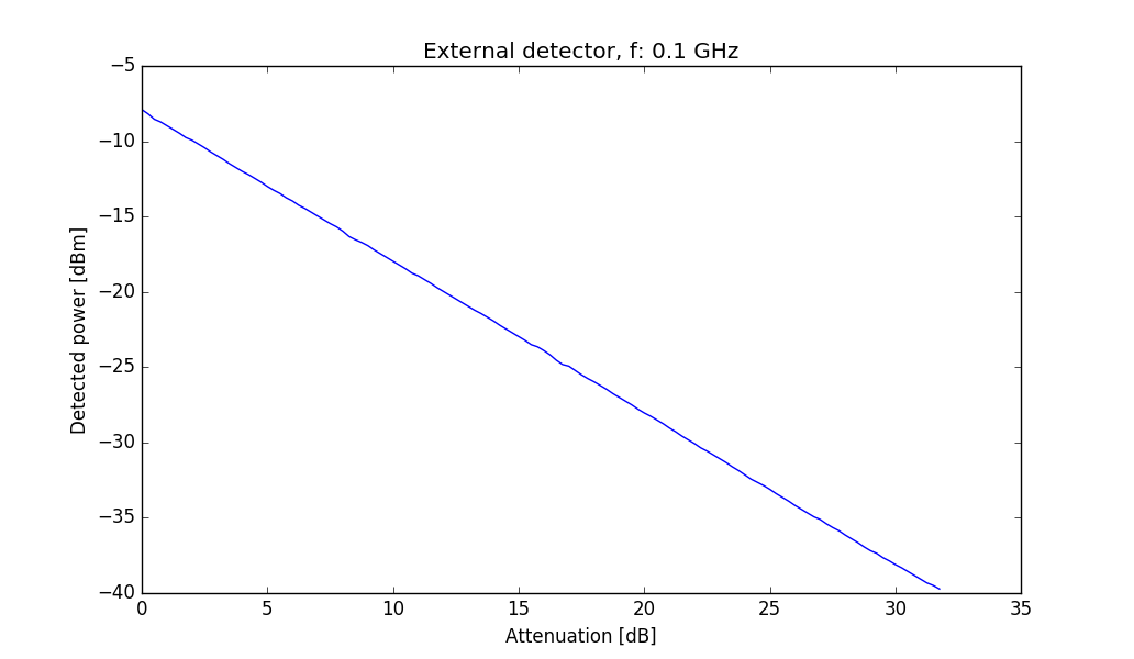
VNA power sweep at 100 MHz measured with power detector. 20 dB attenuator was used at the detector input.
Power detector is connected to the output of the VNA with 20 dB fixed attenuator in between to limit the power to detector. I wrote a quick Python script to step the attenuator values and measure the power at the output of the VNA using power detector. At 100 MHz the linearity seems to be quite good. Since there is a 20 dB attenuator before the power detector, maximum output power of the VNA is about 13 dBm at this frequency.
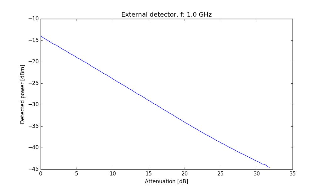
At 1 GHz power output of the VNA drops a little bit and the linearity can be seen to drop a little bit below -40 dBm.
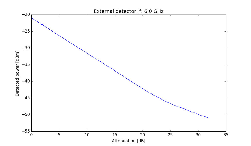
At 6 GHz the output power of the VNA drops further. Now the maximum output power is under 0 dBm. It could be raised few dBm by increasing the output power of the PLL, which was set to medium power setting for this measurement. Below -45 dBm reading starts to significantly deviate from linear.
Input matching
Input matching of the detector chip itself is very high impedance, so the matching suggested by the datasheet is 50 ohm resistor to ground before the detector input. I used the suggested matching on my PCB since I wanted it to have a good matching over wide bandwidth.
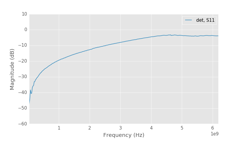
Input reflection coefficient of the power detector measured with my VNA.
While the matching at low frequencies is very good, at high frequencies it quickly becomes very poor. At 4.5 GHz matching is only -3.4 dB.
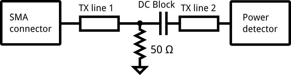
Block diagram of the input matching.
Cause of the poor matching at high frequencies is the TX line 2 before the power detector input. At low frequencies length of the transmission line is electrically short and looking from the SMA detector board looks like high impedance power detector in parallel with 50 ohm resistor, which is close to 50 ohms giving good matching. At high frequencies the transmission line isn't anymore electrically short and when it is 90 degrees long the high impedance of power detector looks like a very small resistance (Transmission line works as a quarter-wave transformer). When a short circuit is in parallel to the 50 ohm resistor, result is still a short circuit resulting in a poor matching.
At 6 GHz 90 degrees long grounded CPW transmission line is about 7 mm long. Trace from resistor to the detector input is about 4 mm long and there are also 1.6 mm tall vias from component ground pad to bottom ground of the PCB. Power detector also has some transmission line inside it from wirebonds inside the package and the total transmission line length is more than 90 degrees at high frequencies.
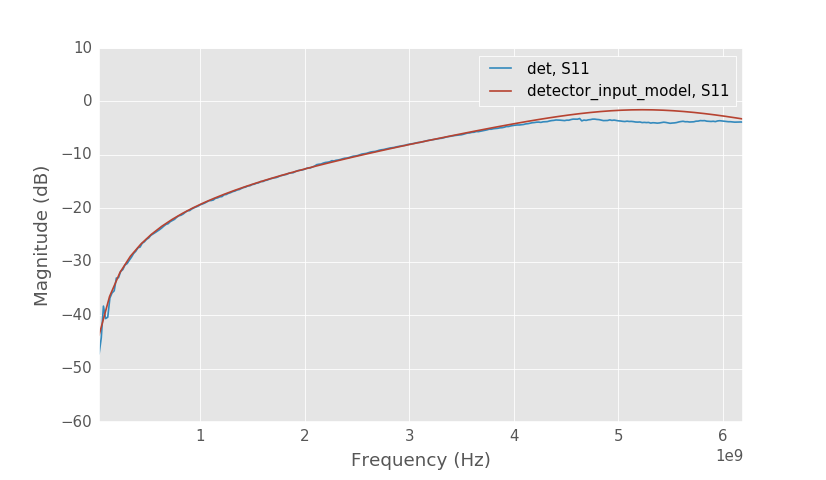
Simulation model and measurement of the input matching.
After fitting the second transmission line parameters to the measured results the simulated input matching agrees very close to the measured matching. Power detector was simulated as 1000 ohm resistance, which is correct at low frequencies. At high frequencies resistance is about 100 ohms which explains the slightly better measured results.

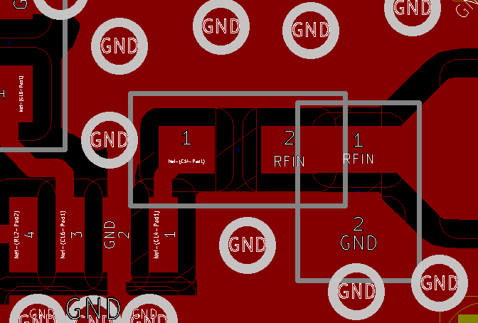
Layout of the RF input.
Looking at the PCB layout of the power detector there are few ways to modify it to improve the matching. Especially RF grounding of the power detector isn't very good. On 2 layer board vias are 1.6 mm tall, which is a long distance at high frequencies. One way to improve the grounding would be to connect top side grounds of the input transmission line to directly to the ground pad of the component. This way ground current doesn't have to go through vias. Although even with this change matching wouldn't still be that good at high frequencies. Input DC block capacitor could also be changed to 0201 package so that 50 ohm resistor can be mounted closer to the input.
Improved layout.
In above picture the grounding of the component is improved by connecting the top side ground to component ground pad (Both sides of the pin 1).
Scalar network analyzer
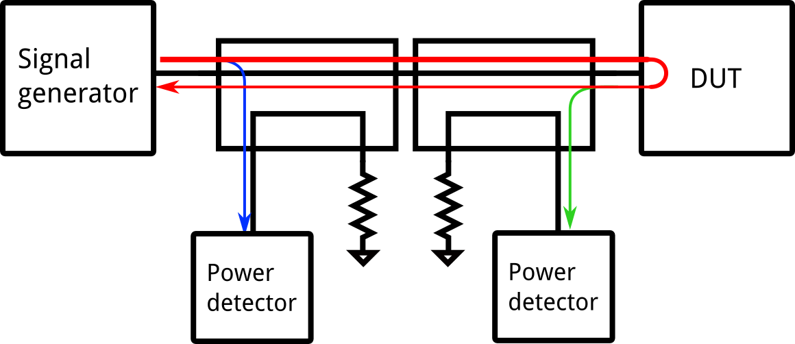
Scalar network analyzer block diagram.
Using two directional coupler, two power detectors and RF signal source a scalar network analyzer can be made. Two directional couplers are connected so that other measures output power of the signal source and other measures the reflected power from the device under test. Ratio of the reflected and transmitted power gives the reflection coefficient of the device being tested.
I don't really need a scalar network analyzer since I have a VNA that has much better accuracy. It is however a nice project and I have all the necessary parts to make it already, so why not?
Similarly to the VNA I made before it can be used to measure reflection coefficient of the device under test. Difference between vector and scalar network analyzer is that scalar network analyzer can only measure the magnitude of the reflection coefficient while vector network analyzer can also measure the phase of the reflected signal. Measured phase can be used to calibrate the instrument enabling it to measure with much higher accuracy, as the scalar network analyzer can't measure phase it can't be calibrated the same way VNA can be and as a result it isn't going to be as accurate.
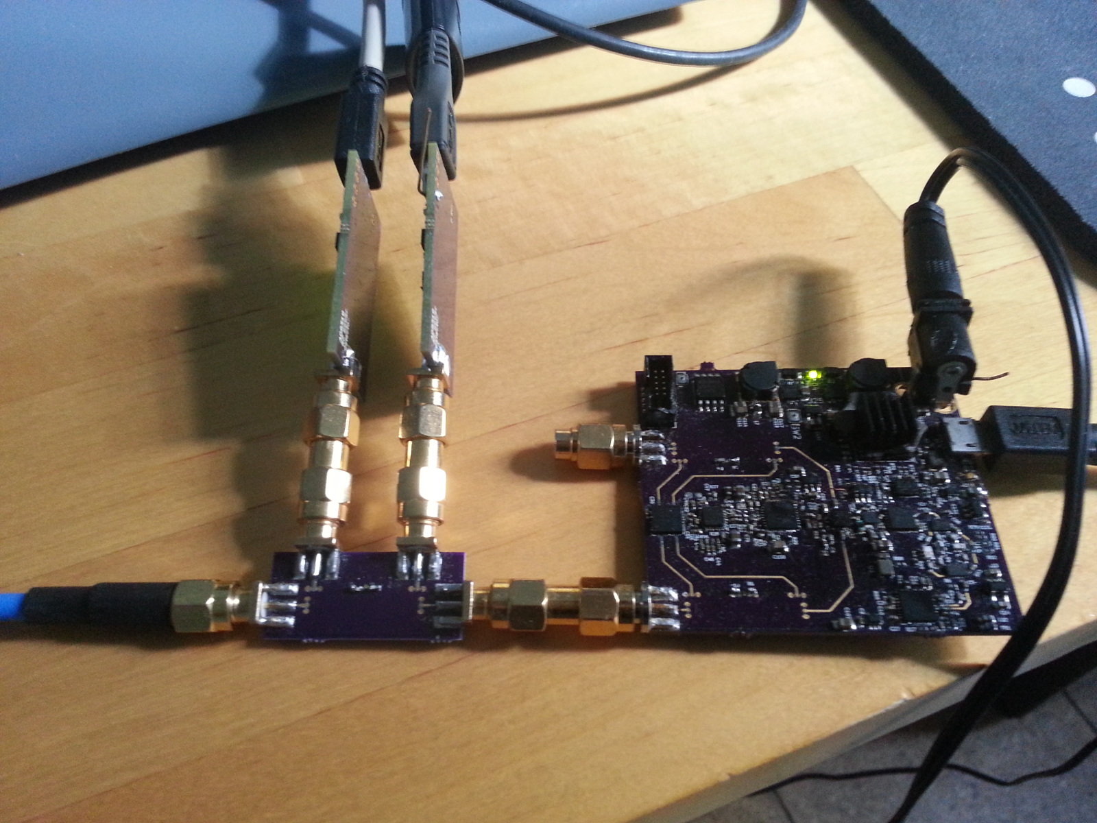
Scalar network analyzer connection.
I have already made a double directional coupler board with the same directional coupler that was used in my VNA. VNA can be used as a signal source and of course the power detectors are the ones I have just made.
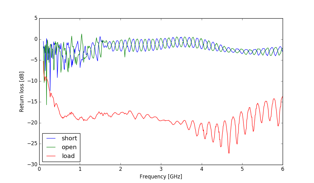
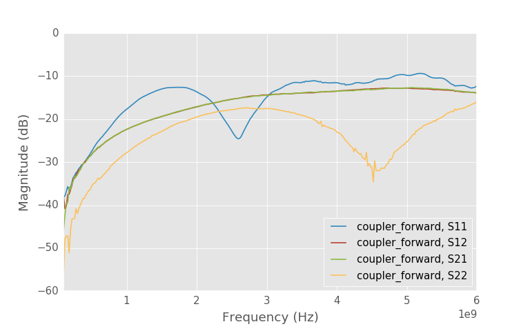
Load, open and short measured using scalar network analyzer.
Above are measured results of short, open and load. Ideally open and short would be straight lines at 0 dB and load would have very low reflection coefficient. Clearly this is not the case here and especially short and open aren't straight lines, but instead have high ripple on them.
Directivity of the directional coupler is about 20 dB, which means that transmitted power going through the directional coupler measuring the reflected power will couple to the power detector with level of 20 dB less than if it would be going the right way. This means that even if the DUT absorbs the signal perfectly without reflecting anything, reflected power is measured to be 20 dB below the transmitted power due to directivity error. This is exactly what is observed when measuring the load.
Ripple in short and open measurements is also caused by directivity error of the directional couplers. Some of the transmitted power from signal source is coupled to the power detector measuring the reflected power and some of the reflected power is measured by the power detector measuring the transmitted power. If the right way coupled and wrong way coupled signals are in phase they will add up and power detector measured bigger power than without the directivity error. If the phases are opposite, signals partially cancel and measured power is lower. As the phase of the reflected signal varies as a function of frequency it causes the observed ripple pattern on the plot.
Measured S-parameters of the coupler board from input to coupling port.
At low frequencies the open and short measurements are very noisy and load seems to have very poor matching. These are caused by the too low coupled power to the power detectors. Coupler board I'm using has low coupling at low frequencies and dynamic range of the power detectors isn't good enough to measure the low power and it shows the noise floor.
Ideal open and short have reflection coefficients of 1 and -1. All of the power is reflected and phase difference between them is 180 degrees. When average of short and open measurements is taken the directivity error is cancelled. As the standards have high reflection coefficient and they don't absorb any power, their averaged measurement measures the losses in the measurement system. Subtracting the average of open and short measurements from other measurements can then be used to correct for the losses in system. It will also correct for the mismatch in sensed power of the two power detectors.
Reflection tracking error calculated from the previous measurements by averaging open and short measurements.
Same measurement as above, but with reflection tracking corrected.
Even with the reflection tracking corrected, ripple on the traces doesn't go anywhere because directivity and matching errors remain uncorrected. Without measuring the phase of the signal they can't be corrected. Accurate measurements using scalar network analyzer require good directivity and good matching from all the components.
Measuring SMA dipole antenna
In order to have something to test the scalar network analyzer with I made a simple half-wave dipole antenna by soldering two wires on SMA connector. Target frequency is 2 GHz, which means that the length of the quarter-wave long wires should be about 37.5mm. Really the wires should be little shorter due to gap between the wires on connector increasing the antenna length by few mm. Thickness of the wires also causes some electric field to fringe also to the ends of the wires increasing their electrical length. It's expected that resonance frequency is little lower than 2 GHz due to these effects.
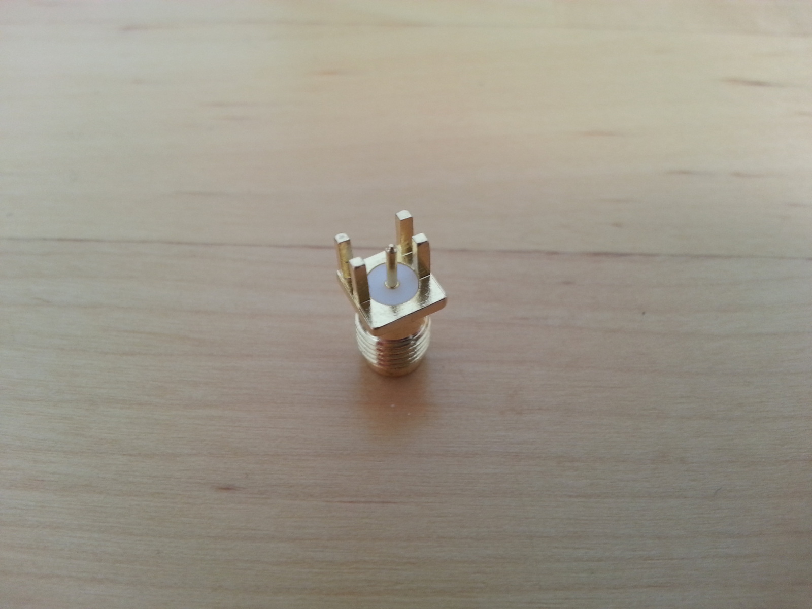
End-launch SMA connector from China. Not very high quality.
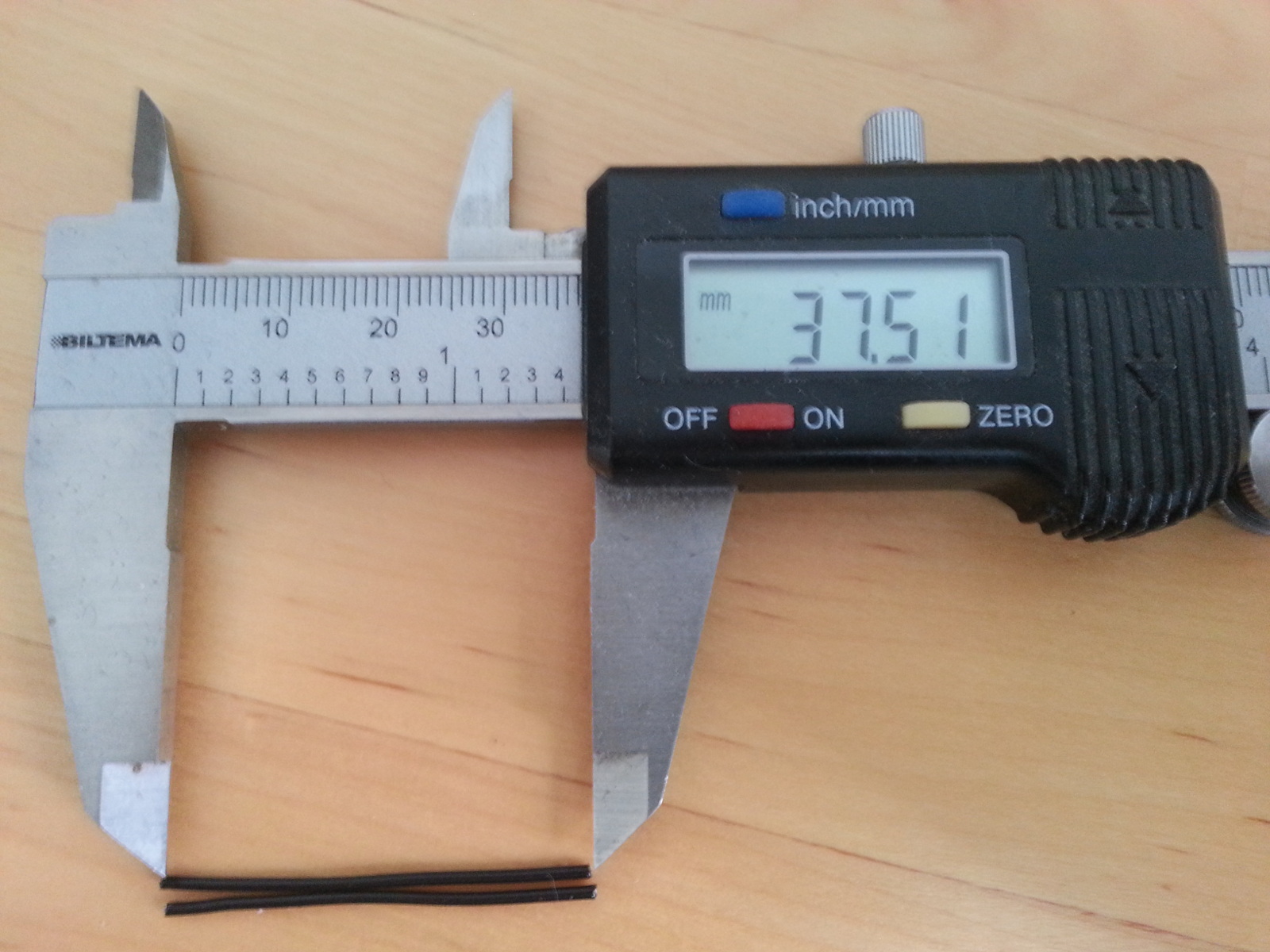
Wires are ordinary single-core copper wire.
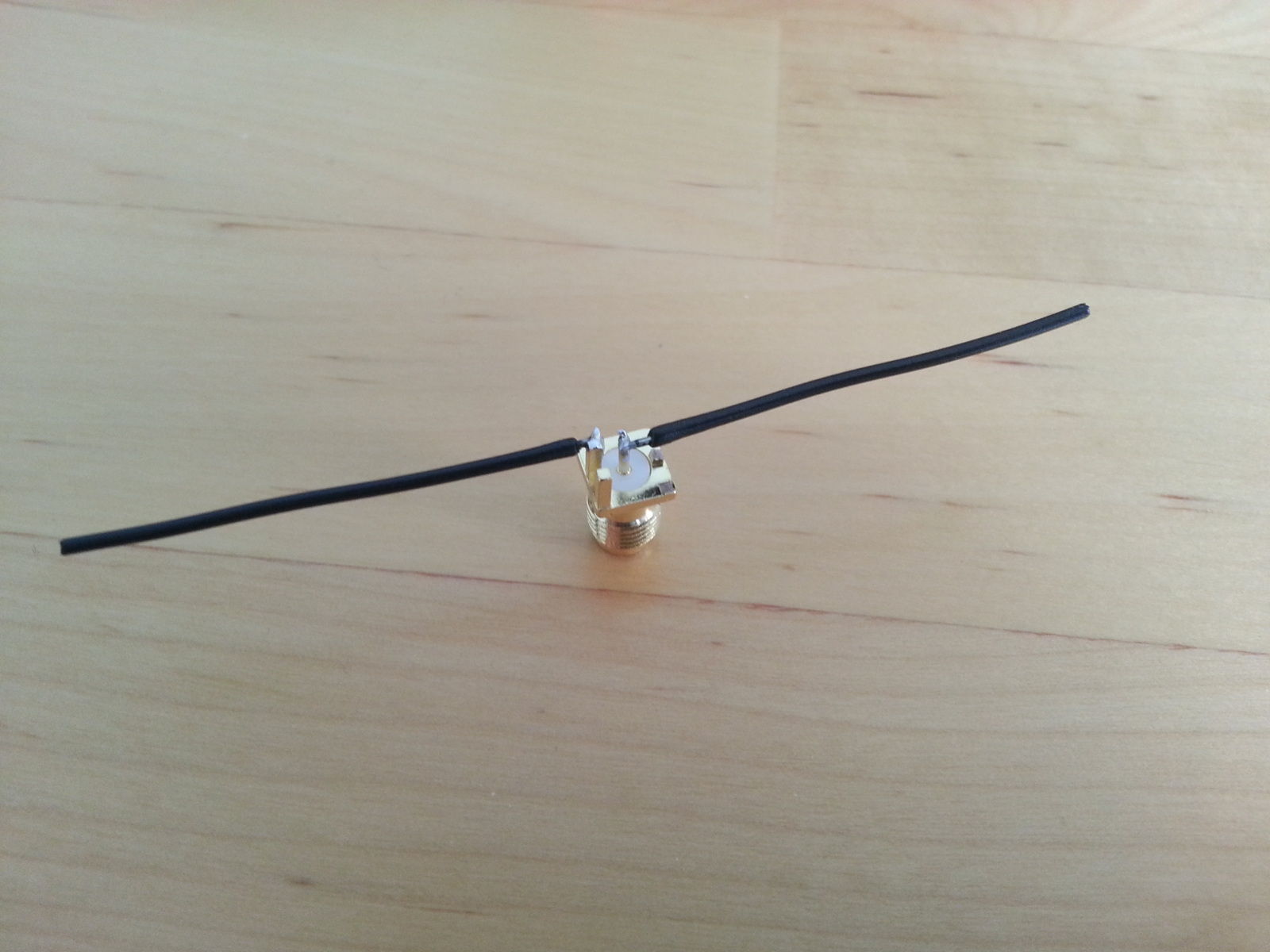
Finished SMA dipole antenna.
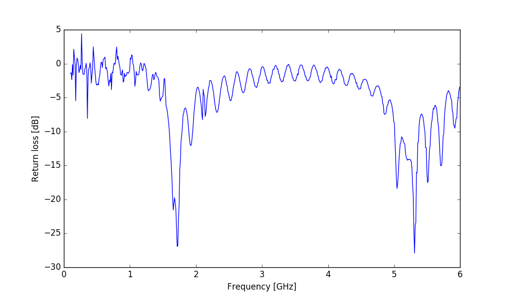
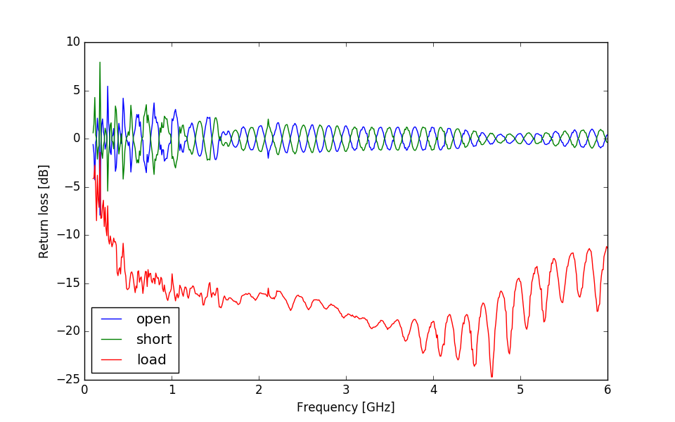
Measured return loss of the SMA dipole.
Measuring the return loss with the scalar network analyzer connection described above gives the above plot of the return loss. While the quality of the measurements isn't very good it can be seen that there seems to be resonance little below 2 GHz as expected and also other resonance around 5.5 GHz.
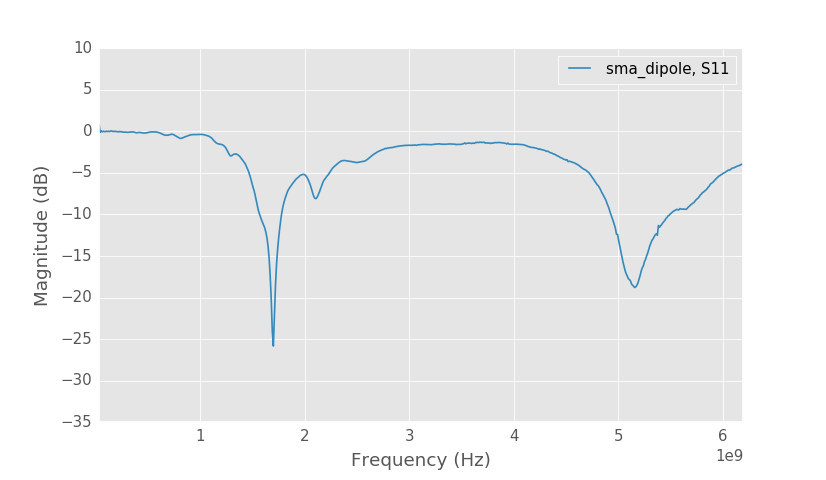
SMA dipole measured with VNA.
For comparison above is the same SMA dipole measured with my VNA. Even though it has similar directional coupler used with the scalar network analyzer measurements, results are much better because of vector error correction allows correcting for the matching and directivity errors.
Conclusion
Power detectors seem to work as designed except that input matching isn't very good at high frequencies. Absolute accuracy is questionable as I don't have a reference to compare it to.
Scalar network analyzer can't really compare to vector network analyzer. It can be made for much cheaper though and could be good enough for measuring antennas for hobbyist use.
You can find the hardware drawing, firmware and PC software on GitHub.