Finished radar boards without antennas.
Introduction
Previously I made a simple frequency-modulated continuous-wave (FMCW) radar that was able to detect distance of a human sized object to 100 m. It worked, but as it was made with minimal budget and there was a lot of room for improvement.
FMCW radar working principle

FMCW radar block diagram
If you have read my previous articles you should know how FMCW radar works, but for completeness sake short explanation is given below:
Frequency Modulated Continuous Wave (FMCW) radar works by transmitting a chirp which frequency changes linearly with time. This chirp is then radiated with the antenna, reflected from the target and is received by the receiving antenna. On the reception side the received signal that was delayed and undelayed copy of the transmitted chirp are mixed (multiplied) together. The output of the mixer are two sine waves that have frequencies of sum and difference of the waveforms. The frequencies of the received signals are almost the same and the sum waveform has frequency of about two times of the original signal and is filtered out, but the difference waveform has frequency in kHz to few MHz range. The difference frequency is dependent on the delay of the received reflection signal making it possible to determine the delay of the reflected signal. The electromagnetic waves travel at speed of light which allows converting the delay to distance accurately. When there are several targets the output signal is sum of different frequencies and the distances to the targets can be recovered efficiently with Fourier transform.
Issues with the previous version
The biggest issue with the previous version was noisy power supplies causing spurs in the received signal, ADC sampling clock not being locked to PLL reference clock and microcontroller being too slow.
To save money I had chosen to use two buck converters to power all the digital and analog components. Even though I chose the switching frequency of the converters to be above the IF frequency, there ended up being some spurs also at lower frequencies. Adding capacitance and swapping the inductors for better shielded ones helped the problem but didn't completely solve it. The proper fix is to add linear regulator after the buck converters to clean up the switching noise.
The problem with separate clocks for ADC and PLL caused the sampling interval of the ADC to vary between separate sweeps. The maximum offset was only +- half a sample and it wasn't a big issue when only doing range measurements. However when trying to measure heartbeat and respiratory rate the added phase noise from the varying sampling interval caused some noise in the measurements. Noisy power supplies also degraded the phase noise performance. The fix for this one is pretty easy: Use the same clock for both ADC and PLL.
The microcontroller I was using was pretty powerful compared to the cheapest 8-bit microcontrollers, but it was hopelessly underpowered to do any kind of digital signal processing. All of processing power and internal memory was spent in getting the samples from ADC to PC through USB fast enough. Sampling speed of the ADC was 10 MHz and because of lack of DSP resources every sample needed to be transferred to PC. Even the samples between the sweeps that didn't have any useful data were transferred to PC only to be discarded later. With more resources it would have been possible to do digital filtering, lower the sampling speed and only transfer the useful samples.
Microcontrollers don't really have enough processing power to do any kind of non-trivial filtering. For example a 100 tap FIR filter requires 100 multiplications and 100 additions for every sample. Even if the multiplication could be done in one clock cycle the maximum sample rate is too low to be useful. The microcontroller should also have enough processing power to transfer ADC samples and do communication and other logic. FPGA works much better for DSP as the operations can be done in parallel.
The last improvement is adding a second receiver antenna. When there are more than one receiver antenna it is possible to determine the direction of arrival of the received signal. If the return signal arrives in angle it is received at different antennas at different times. The different arrival time causes a phase shift in the IF signal which can be used to determine the direction.
Link budget
Since I'm not changing the transmitter, the maximum range performance should be pretty identical to the last version when using the same horn antennas. When smaller patch antennas are used as receiver antennas the range is going to decrease because the gain and efficiency of the patch antennas is smaller.
The maximum range to detect a target can be calculated using the radar equation:
where \(P_t\) is the transmitted power, \(G\) is gain of the antennas, \(\lambda\) is wavelength, \(\sigma\) is the radar cross section of the target and \(P_{\text{min}}\) is the minimum detectable signal power.
Most of the values are easy to determine, but the minimum detectable power can be tricky. Clearly the minimum power that can be detected depends on the noise level of the receiver. Noise at the receiver input is RF thermal noise, which can be calculated with \(kTBF\), where \(k\) is the Boltzmann constant, \(T\) is noise temperature, \(B\) is noise bandwidth and \(F\) is the receiver noise figure.
Determining the correct noise bandwidth to be used is critical and easy to get wrong. Noise bandwidth is clearly smaller than the sweep bandwidth since the IF filter filters most of the RF noise out. IF filter bandwidth determines the noise power that makes it to the ADC, but that is not the noise bandwidth to be used since some of the noise can be clearly filtered out after taking the FFT. When FFT is taken of the IF signal the total RF noise is split equally to each FFT bin. Bandwidth of one FFT bin is the noise bandwidth of the receiver and the bandwidth that should be used in the calculation. Bandwidth of one FFT bin depends only of the lenght of the FFT. With FMCW radar FFT length equals length of one sweep, \(t_s\) and bandwidth of one FFT bin is \(1/t_s\).
With sweep length of 1 ms and noise figure of 6 dB the RF noise floor at the receiver input is -138 dBm. For the signal to be detectable it should be some amount more powerful than the noise. Using 20 dB for the required signal-to-noise ratio gives minimum detectable signal of -118 dBm.
| Variable | Explanation | Value |
|---|---|---|
| \(P_t\) | Transmitted power | 15 dBm |
| \(G\) | Gain of antennas | 13 dBm |
| \(\lambda\) | Wavelength | 5.2 cm |
| \(\sigma\) | Target radar cross-section | 1 m² |
Plugging the values above to the radar equation the maximum range that radar can see a human sized 1 m² cross-section target can be solved to be 320 m. The target size does have a big effect, for example a bird sized target with cross-section of 0.01 m² can be detected only below 102 m. The transmitted power in the table is somewhat pessimistic to include losses from antennas, cables and PCB.
This would be correct for radar looking at air, but when the radar antennas are looking at a low angle there is going to be problem with clutter that can decrease the SNR. When angle of the antennas is low and the radar is on a flat ground there is going to be returns from the ground from basically every range. Returns from other objects such as trees, buildings and other objects can also overlap the target signal decreasing the signal to noise ratio.
Receiver design

Simplified radar block diagram.
The previous range calculation assumed that the receiver has sufficient dynamic range to detect the RF noise floor, linearity is good enough. Care should be taken especially with the dynamic range of the receiver since reflections from targets near the antennas are going to have much larger power than the noise floor and the receiver should be able to resolve both returns at the same time.
Noise figure of the receiver should be kept as low as possible which can be done by choosing a low noise amplifier with low noise figure and high gain. Higher the gain of the LNA is the smaller the noise contributions of the following stages. A drawback of having high gain is that the input compression point is lowered as either the LNA output stage, mixer or IF amplifier starts to saturate earlier due to higher output power of the high gain LNA. If the input compression point is too low receiver can saturate just from the leakage power between the transmission and receiver antennas. In saturation the receiver doesn't work linearly anymore and many harmonics are generated that are detected as false targets. It's very important to avoid saturating the receiver and this is one of the major issues when using single antenna that is shared between transmitter and receiver. Radar with a low input compression point has higher minimum detection distance below which the returns from the targets saturate the receiver. Choosing the LNA gain ends up being a compromise between noise and input compression point.
It's important to also take into account the noise figure of the low frequency amplifier driving the ADC and noise floor of the ADC. Op-amps typically can't be analyzed using noise figure because ports aren't matched to 50 ohms. The right way is to convert the RF noise to V/\(\sqrt{\text{Hz}}\). However comparing the input noise voltage density of the op-amp to noise voltage density of 50 ohm resistor gives a close enough value for hand calculations. Usually op-amps have quite high noise figure due to the resistors used to set the gain. NF of ten to twenty dB is usually a good guess.
ADC has quantization noise and input noise that results in limited dynamic range. Datasheet of the ADC lists the SNR which is calculated by measuring a maximum amplitude sine wave, taking FFT and then dividing the signal power by noise power in all other FFT bins. The dynamic range can be increased with oversampling and filtering. The noise floor after taking the FFT is considerably better than the SNR number listed in the datasheet because noise at different frequencies can be separated.
The dynamic range of the ADC with the FFT processing gain can be calculated with:
where SNR is the SNR of the ADC listed in the datasheet, \(f_s\) is the sampling frequency and \(t_s\) is sweep length. LTC2292 ADC that I used has listed SNR of 71.3 dB and sampling frequency is 40 MHz. This gives ADC dynamic range of 117 dB with 1 ms sweep.
To make sure that the ADC doesn't limit the system performance the RF noise floor after the ADC should be above the ADC noise floor. The input referred RF noise power at the LNA input is \(kTBF = kTF/t_s\). This is amplified by the LNA and mixer by \(G_{\text{LNA}}G_{\text{mixer}}\). After the mixer the RMS output voltage can be calculated as \(V = \sqrt{Z_{\text{load}} P}\), where \(Z_{\text{load}}\) is the mixer output impedance (200 Ω on the mixer I'm using). This voltage is amplified by the IF amplifier by \(G_{IF}\). Next the RMS voltage should be converted to peak-to-peak value by multiplying by \(2\sqrt{2}\) and then referenced to maximum ADC voltage range. Finally by taking \(20\log_{10}\) we will get the noise floor in dBFs units (relative to ADC maximum input signal). Putting it all together in one equation gives:
| Variable | Explanation | Value | \(V_\text{ref}\) | ADC maximum peak-to-peak voltage | 2 V |
|---|---|---|
| \(G_\text{IF}\) | IF amplifier gain | 20 dB |
| \(G_\text{LNA}\) | LNA gain | 20 dB |
| \(G_\text{mixer}\) | Mixer power gain | 0 dB |
| \(k\) | Boltzmann constant | 1.38064852×10⁻²³ m2 kg s-2 K-1 |
| \(T\) | Noise temperature | 290 K |
| \(Z_\text{load}\) | Mixer output impedance | 200 Ω |
| \(F\) | Receiver noise figure | 6 dB |
| \(t_s\) | Sweep length | 1 ms |
Plugging the above values into the equation gives the noise floor as -102 dBFs. This is 15 dB over the ADC noise floor and the receiver performance is not limited by the ADC.
FPGA Digital signal processing

Block diagram of FPGA DSP.
ADC sampling speed is fixed at 40 MHz, but this is much more than needed. IF filter bandwidth is only 2 MHz so from about 2 MHz to 40 MHz there is only noise which should be filtered out. The reason for such high sampling speed is avoiding aliasing and SNR increase from oversampling. Sampling rate needs to be dropped to make the amount of data manageable. Without decimating the data rate would be 120 MBps, which exceeds the USB 2.0 datarate and is very challenging to store anywhere. Dropping the sample rate to 2 MHz and increasing bit resolution to 16 bits results in much more manageable 8 MBps data rate. When samples between the sweeps are dropped the data rate further reduces by ratio of sweep length to time between the sweeps.
Data rate reduction could be obtained by reducing the ADC sampling speed or dropping some of the ADC samples, but these methods don't get the SNR gain from the oversampling. Averaging of the samples could be used, but this corresponds to filtering with FIR filter with constant 1 coefficients and is not spectrally very nice and will cause aliasing. The correct way is to use FIR filters to filter out the frequencies that would alias and then decimating (dropping samples). This method will give the SNR improvement from oversampling and avoids aliasing of higher frequencies.
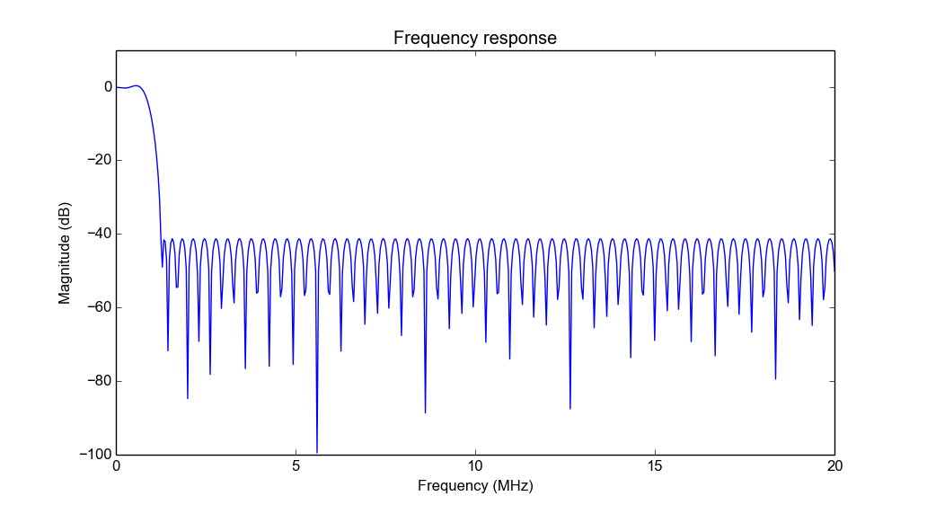
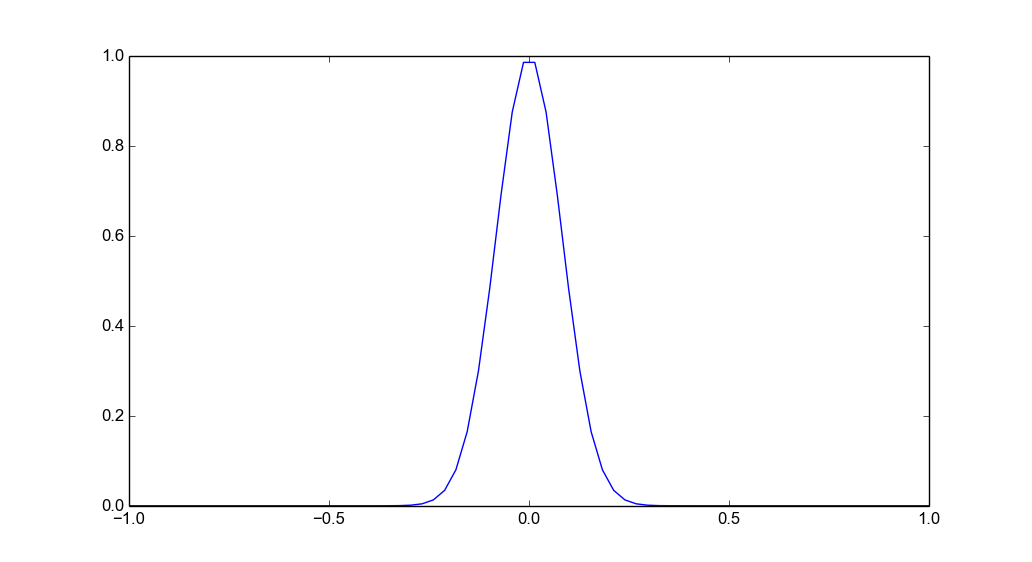
Frequency response of the first FIR filter.
Big advantage of digital filtering compared to the analog filtering is that it can be made as accurate as needed, it's noiseless and doesn't require any additional hardware. Above is the frequency response of the first 120 tap FIR filter in the block diagram. This high order would be infeasible to make using analog components but digitally implemented it's not a problem. By combining the decimation and filtering the implementation can be made much more efficiently compared to the naive implementation. High order filter has advantage that transition band can be made very small thus resulting in less wasted spectrum.
The two channel 120 tap FIR filter needs 10 DSP slices when decimating at 20. The other filters are implemented as one filter with reconfigurable coefficients and only require 2 DSP slices. All the filters need a total of 12 DSP slices out of 45 available DSP slices on the FPGA I'm using. Amount of DSP slices required could be dropped even further by increasing the clock speed, but there is no need for it since there is still plenty of room left.
Beamforming

Antenna array.
Two antennas receiving a reflection from the same target will have slightly different phase shift on the received signal due to the small angle dependent difference in the distance to the target. The path length difference between the antennas is \(d\sin\theta\), where \(d\) is the distance between the antennas and \(\theta\) is angle of the target. Phase shift of the received signal is \(d\sin\theta/\lambda\) where \(\lambda\) is the RF wavelength.
If the antenna outputs are just summed together the targets straight ahead will sum in the same phase while the targets from angle where \(d\sin\theta/\lambda= -1\) will be summed in the opposite phases and will cancel each other. Angles between these extremes will experience different degrees of interference.
Beam forming can be done by phase shifting the signals before summing them. When the phase shift \(\phi\) is chosen such that \(\phi = -d\sin\theta\) the peak of the antenna pattern is shifted to angle \(\theta\).
To generate multiple beams for generating an image the simple way would be to repeat the summing of signals for different phase shifts. A more efficient way to synthesize multiple beam is possible using Fourier transform. For radar signals we want to first take FFT of the each ADC signal to move to frequency domain. Each bin of the FFT corresponding to different distances has amplitude and phase of the echo signal. Next all the Fourier transformed signals are placed in array and a second FFT is taken across the antenna dimension. This is equivalent to summing the signals with different phase shifts. Zero padding the array before taking the FFT is necessary to get some resolution to the output. Otherwise we would only get same number of beams as there are antennas.
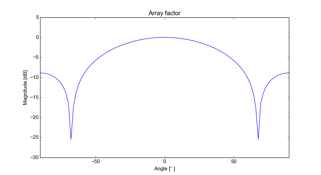
Array factor with two antennas.
Above plot is the array factor of the two antenna array. This is the beam pattern assuming that the antenna patterns is omnidirectional. The pattern of the real array can be calculated by multiplying the array factor with the radiation pattern of single antenna.
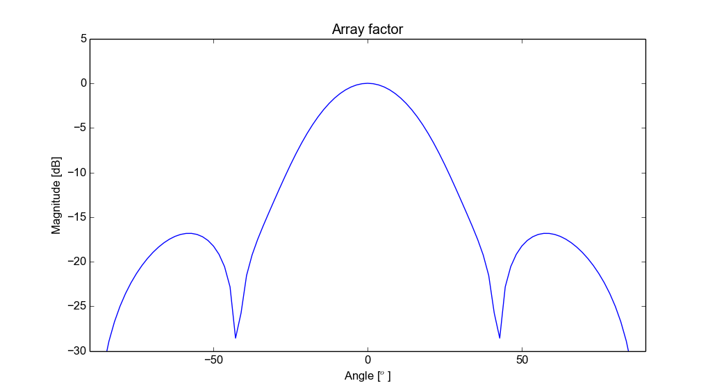
Array factor with eight antennas. Hamming window weighthing.
With eight antennas the angle resolution would be much better and of course even more antennas would give even better angle resolution. Eight receiver channels would increase the cost and power consumption by quite a bit, but it would be possible to have eight antennas that are connected to two receiver channels with a switch. All antennas could then be sampled in four separate sweeps.
Because the array beam width with only two antennas is so poor it's hard to see the angle information on the plots. The angle visualization can be improved by multiplying the measurement with a windowing function that is shifted to the peak location. If there is only one target in the range bin it works well, but if there are multiple targets then the peak is somewhere between them and the windowing makes it look like that there is only one target. There are issues especially with walls and other very wide targets that are reduced to one target by the windowing.
Angle windowing function.
Designing PCB
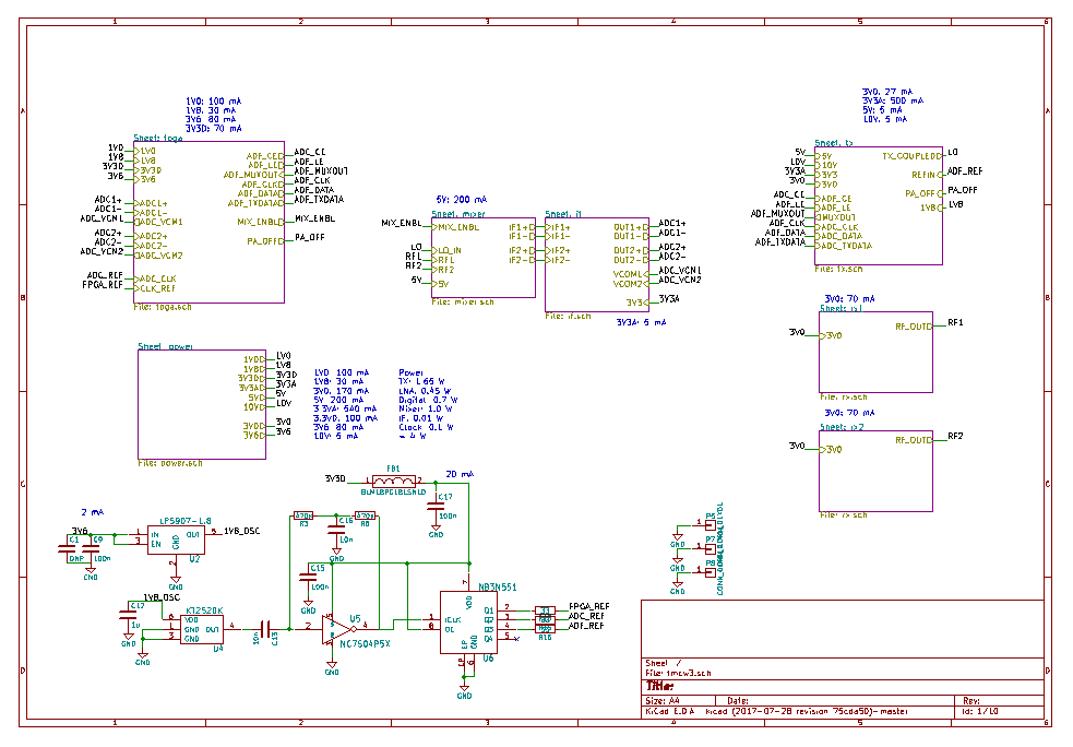
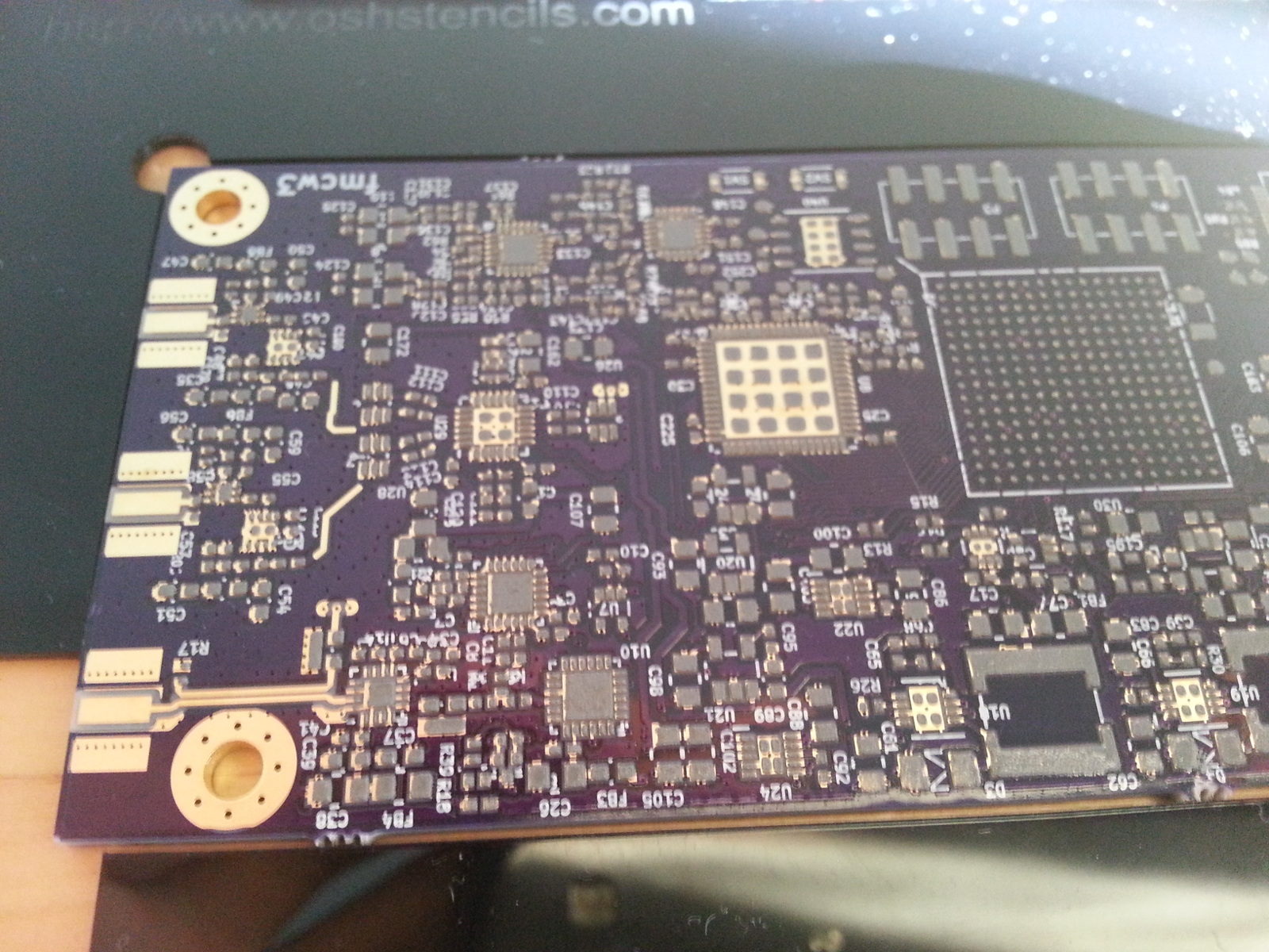
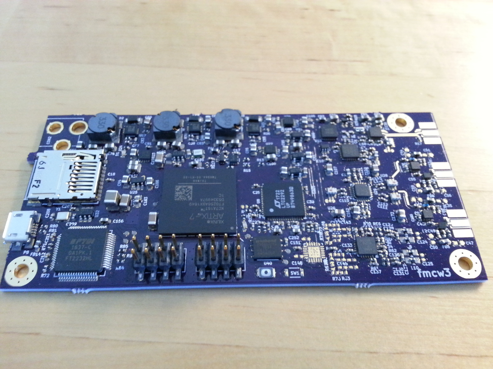
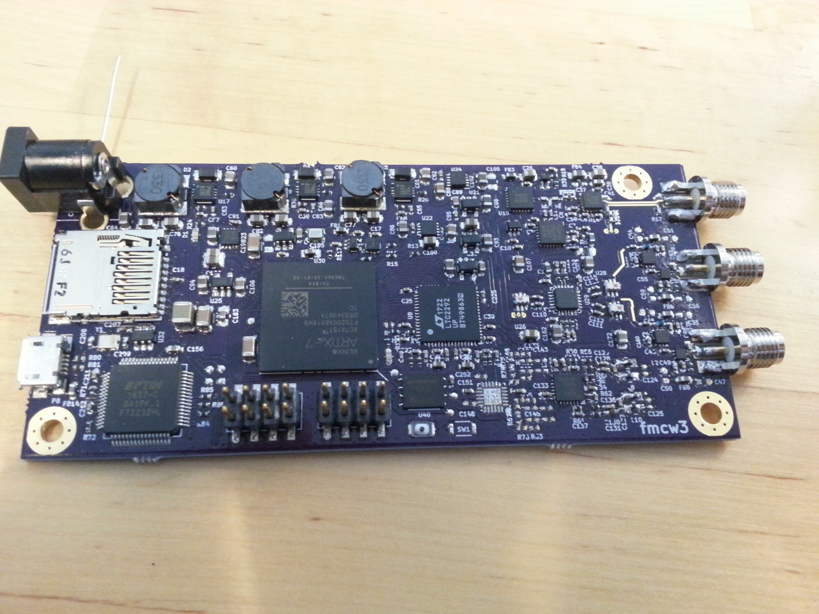
The PCB was designed for the same OSH park 4 layer process that I have used many times with my earlier projects. It is the only cheap PCB manufacturing process with better material than FR-4. The material is FR408 which is like FR-4, but losses are lower and the relative permittivity is more tightly controlled.
Compared to the previous version the PCB is much bigger. Especially the FPGA requires a huge amount of space. Power supply is more complicated because FPGA requires several voltages and there are now several linear regulators on board to clean up the switching noise. Of course the second receiver channel also takes lot of space.
Some things however are simpler than before. Previously the IF filter had several op-amps and had variable gain. Now there is only one amplification stage, because I actually calculated that multiple stages are not needed. Variable gain has also been removed and instead ADC dynamic range is maximized so that there is enough dynamic range to not need it.
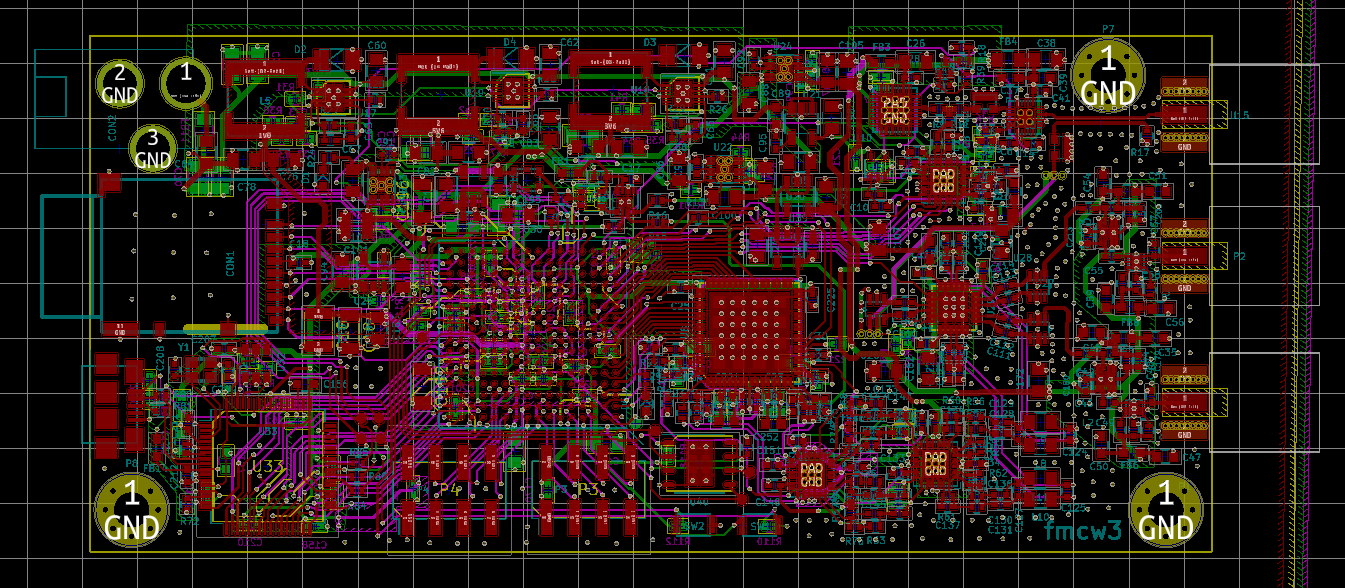
Layout in KiCad.
I placed an SD-card holder on the PCB for use without a PC but I haven't actually programmed the FPGA to use it yet. There are also two headers that are connected to FPGA IO pins. I don't have any definite use for them, but some examples I had in mind are connecting an inertial measurement unit for SAR motion correction, connecting control signals for use without PC and controlling external antenna switches.
Soldering
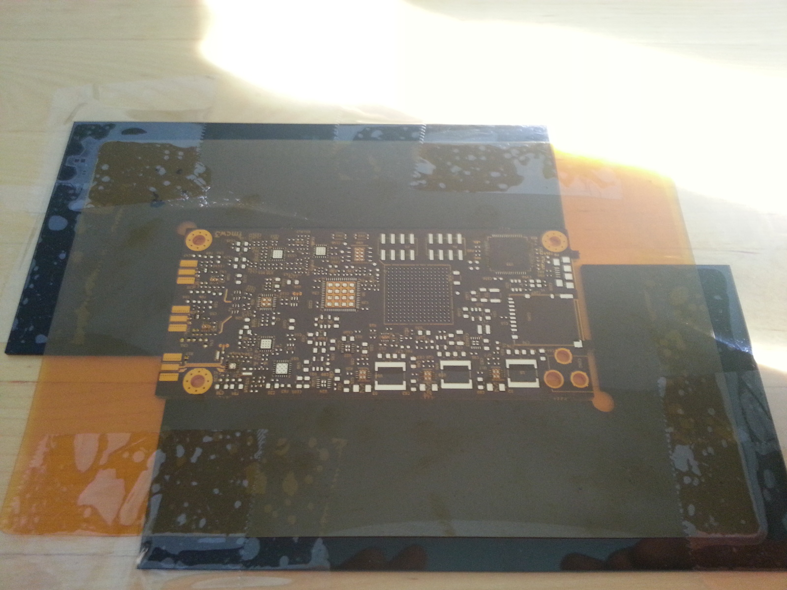
Applying solder paste with stencil.
Although I tried to keep the PCB simple it still ended up having about 350 components and many of them are in hard to solder packages.
I start with the more complicated top side. I used to solder the bottom side first with some of the previous projects, but it's easier to apply the solder paste on the top side when there aren't any components on the bottom side. The solder paste is applied using a stencil from OSH stencils. I bought a cheaper Polyimide stencil this time instead of more expensive stainless steel one and I have to say that the stainless steel stencil works much better.
Solder paste on PCB.
Components placed on paste.
The empty QFN footprint on the bottom right is for a second IF amplifier stage. I added it just in case, but didn't end up needing it.
After soldering and adding connectors.
Like all my previous projects I soldered the PCB myself using my reflow oven.
Quality wasn't perfect this time and I had to fix some components by hand later.
When there are so many components there are bound to be some that don't get soldered correctly. One of the components was soldered incorrectly probably due to uneven solder paste placement. I fixed this component by hand using hot air.
Antennas
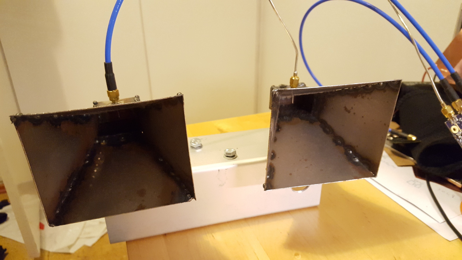
The old horn antennas I made previously.
I have the horn antennas that I made previously, but there are only two of them and they are not very suitable as receiver antennas due to their large size. Because the antennas are large they need to be placed far away from each other. When distance between the receiver antennas is more than \(\lambda/2\) the phase shift of the received signals exceeds 180 degrees for some angles. The resulting IF signal is identical to some smaller angle causing aliasing.
Patch antenna
To avoid angle aliasing I made new patch antennas that are placed \(\lambda/2\) away from each other. Due to budget constraints, the PCB material is ordinary FR-4. It has high losses at RF frequencies and causes the antenna to have low efficiency. Relative permittivity of the FR-4 is not very well controlled and varies between the manufacturers and different manufacturing runs. Change in the relative permittivity results in shifting of the antenna operating frequency. Unfortunately any better materials are much more expensive. FR-4 PCBs can be had for less than 10 € from China, while the same PCBs with better material would cost at least 100 €.
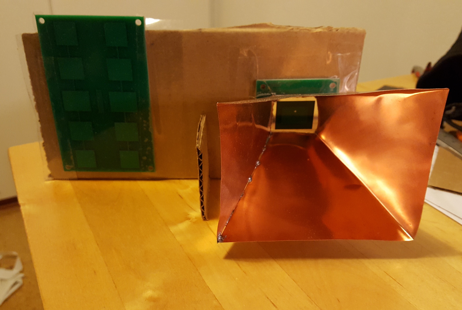
2x5 patch array (left) and patch fed horn (right). The thin copper sheet horn has taken some damage.
The antenna consists of five patch antennas in a line with the center antenna being fed from SMA connector through a via underneath the board. Compared to a single element patch antenna the five element array radiates much less in the direction of the array, while in the other direction beam width is very similar to one element patch antenna. The antenna is meant to be mounted such that in the horizontal plane there is a wide beam width for good angle coverage and narrow beam width in the vertical direction to minimize the ground returns.
I also made a horn antenna fed by a patch element. Compared to the previous waveguide fed horn antennas the operating bandwidth is much smaller and the efficiency is lower. The advantage is that the construction is much simpler and the antenna is much easier to mount because of its flat bottom side.
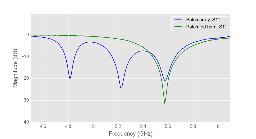
Measured patch array and patch fed horn S-parameters.
The measured S-parameters of the antennas look good except that the operating frequency has shifted to lower frequencies. The design frequency was 5 GHz ISM band (5.725 - 5.875 GHz), but the realized operating frequency of the manufactured antennas is about 150 MHz lower. The reason for the frequency shift is different relative permittivity of the substrate material in simulations and manufactured antennas. I made one patch antenna on FR-4 before and I measured that it had relative permittivity of 4.20 which I used for simulating the new antennas. However based on the measurements FR-4 on the new antennas has relative permittivity of about 4.58.
Measurements
Noise floor
Attenuators on transmitter and receivers.
Earlier I calculated that the RF noise floor should be about -102 dBFs. The noise floor can be measured easily by attaching attenuators to transmitter and receiver. ADC noise floor is harder to measure because I can't disable or disconnect the receivers. I could desolder some components or add a short circuit, but I'm not going to bother.
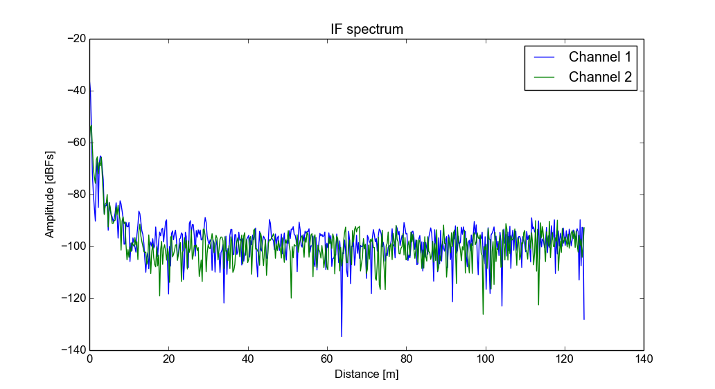
Above is the measured receiver power spectrum in dBFs (relative to the maximum ADC input voltage). Calculation was -102 dBFs and the measurement is -99 dBFs on the first channel and -100 dBFs on the second one. Measurement agrees very well with the calculation considering that the gains of the components can vary few dB.
At low frequencies/distances there is some signals visible. The lowest bin is DC and is probably caused by the IF amplifier and ADC DC offset and FFT windowing. At little bit higher frequencies there are some genuine targets probably from ceiling and walls. If I wave my hand over the radar I can see the targets moving. It seems that the microstrip lines on the board radiate enough that radar can detect some nearby targets without antennas. A similar issue could be seen with my homemade VNA. Unlike with the VNA, isolation is not too important with FMCW radar because it will only cause targets at very low distances.
Park
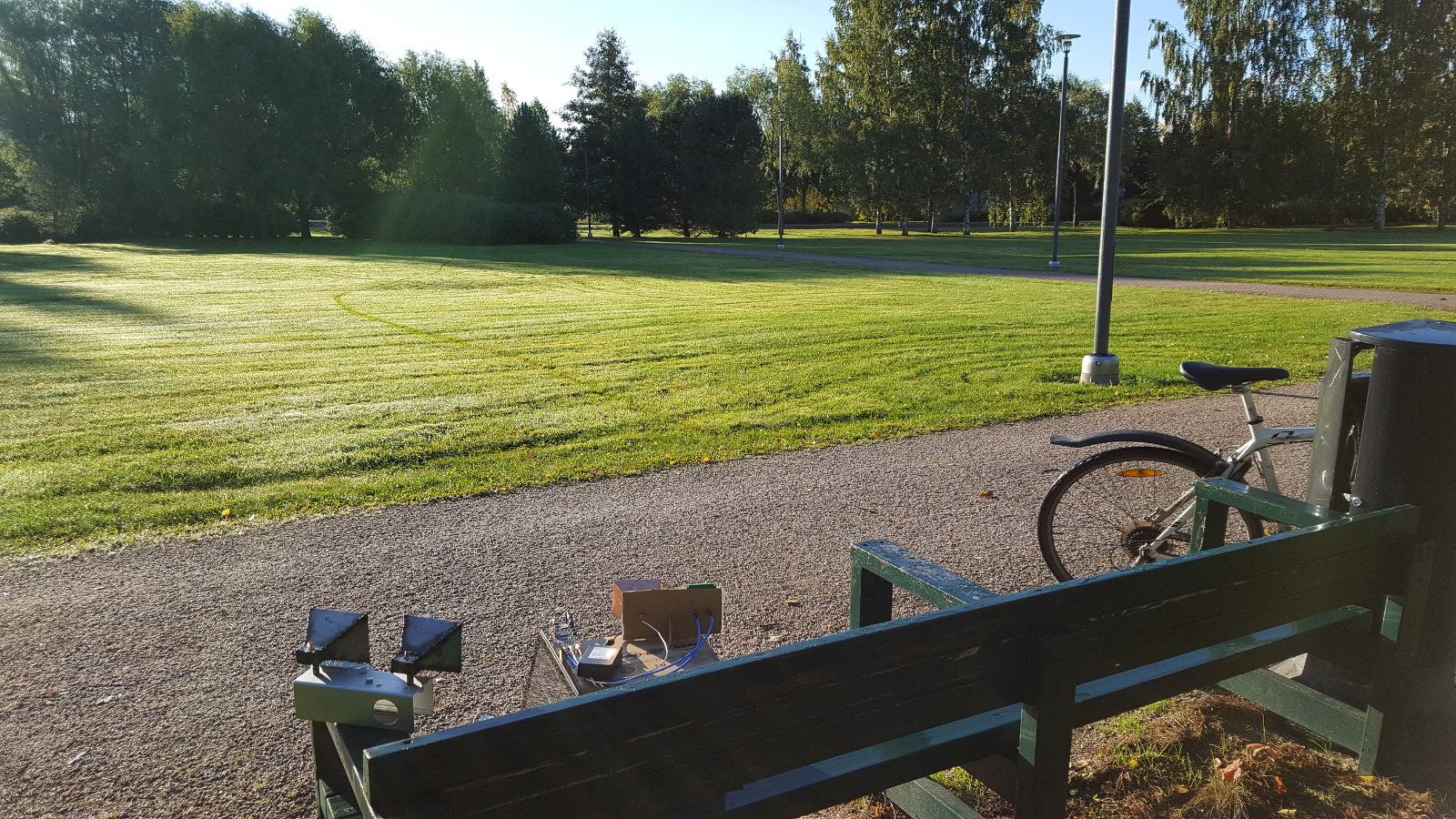
Image of the scene.
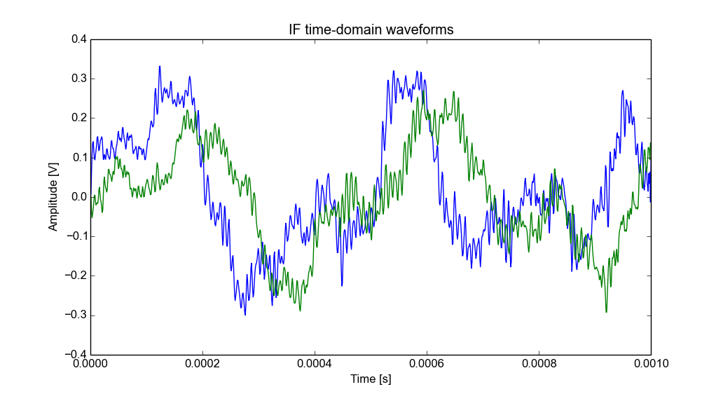
Time-domain plot of the received signals.
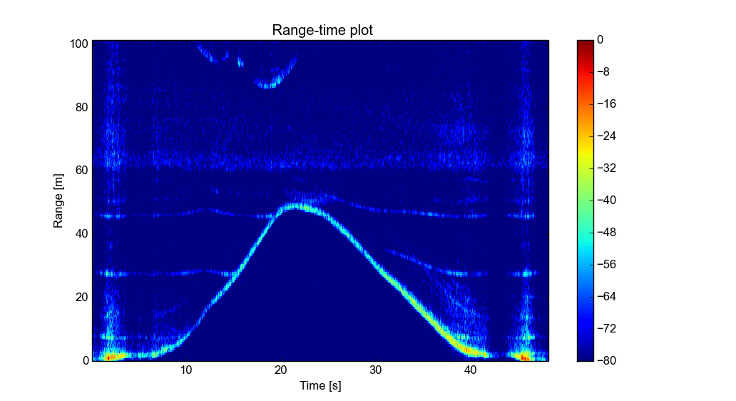
Time-range plot captured with the patch antennas. Previous sweep is subtracted from the current one to remove fixed targets.
Above is a time-range plot of me riding a bicycle in a circle in front of the radar. The circle part of course is not visible on this plot as angle of the target is not shown.
With the added angle dimension visualizing the data now requires a video. Above is a video of the same measurement that was plotted above. This time fixed targets were not removed and lightning posts and trees are visible as fixed targets. Without the angle information the fixed targets would have just cluttered the plot but now the video looks quite clear even without any additional post processing.
You can tell from the video that I start and end the video at left side of the radar (positive cross range). Walking in front of the radar at the beginning shadows the background targets and also causes some clipping at IF due to the strong reflections.
The angle resolution is not that good but this is expected because there are only two receiver antennas. Windowing used for visualizing the angle of target causes the wide bushes at the background seem to oscillate wildly because of small changes in the received reflections. Because returns at different angles are nearly equal small noise can flip the peak to different location.
In the video it's clear that magnitude of reflections around the center is much bigger than at the edges. This is mostly because of the narrow beam width of the transmitting horn antenna. Receiver antennas will also have less gain at high angles further dropping received reflection magnitude.
The lamp posts in the picture are also clearly visible on the video and don't move around as much as the bush. When I go near them in the same range bin the location seems to jump around. The problem is that when I am at the same range as them the angle windowing still assumes that there is only one target and puts the target center somewhere between the lamp post and me.
Above is the same video as previously, but with the previous sweep subtracted from the current one to remove fixed targets. Subtracting the fixed targets highlights some of the problems with the angle visualization even more.
Traffic speed
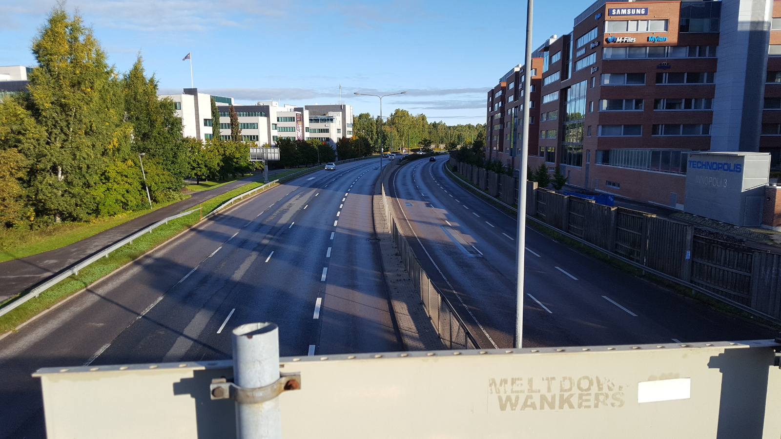
Image of the scene.
There was a nice bridge near me that went over a busy road so I decided to test how well the radar can see cars. Cars are have pretty big radar cross section and should be visible very far.
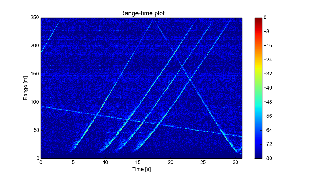
Time-range plot of traffic with fixed targets removed.
The above time-range plot is recorded with a single horn antenna so there is no angle information. Clutter is removed by subtracting the previous sweep from the current one leaving just the moving objects. Without the clutter reduction there are so many targets that it's hard to see anything.
The range was previously cut off because there wasn't any far away targets, but this time I'm plotting the full range. Decimate by two filter was active during this capture to limit the data rate and it limits the range to 250 m with 300 MHz sweep. Without decimating the range would be 500 m, but there isn't much point in capturing that since the line of sight from the bridge is less than that. SNR is still good at 200 m so it should be able to see much farther. At far ranges the drop in SNR is caused by the decimation filter filtering also little bit below the Nyquist frequency to avoid aliasing.
From the plot it can be seen that during the capture there five cars going away from the radar and one car and one bicyclist coming towards. Car speeds can be calculated from the graph by simply dividing the traveled distance by time it took to travel it. There are better ways for measuring the speed, but I'm too lazy to implement them. The solved speeds are around 60 to 70 km/h. The speed limit is 80 km/h so all of them seem to be driving little below the speed limit, but I guess that makes sense as there are traffic lights just after me.
Conclusion
The changes in the newest version fixed the problems in the previous version and the performance of the radar seems very good. Two receiver channels allows determining the angle of the target, but the angle resolution with only two receiver antennas is not too good. The angle resolution is limited by the physics and getting more resolution would need more antennas. Multiple switched receiver antennas are on my todo list.
If you are interested in taking a more detailed look, all hardware design files, firmware and processing software are available at github.