Introduction
I have been using the OSH Park's 4 layer process a lot on my own projects. It has FR408 substrate that has better controlled permittivity and lower losses than ordinary FR-4 that other low cost PCB manufacturers use. In my opinion currently it is the best low cost process for making RF PCBs.
My previous boards have worked pretty well, but I decided to make a test board that I can use to characterize the process better.
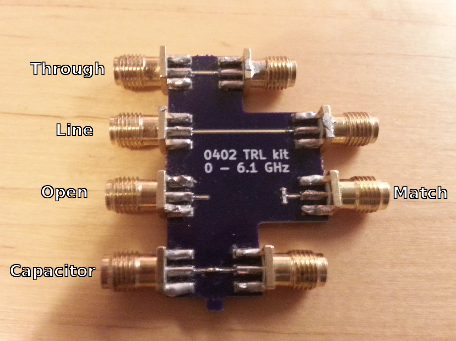
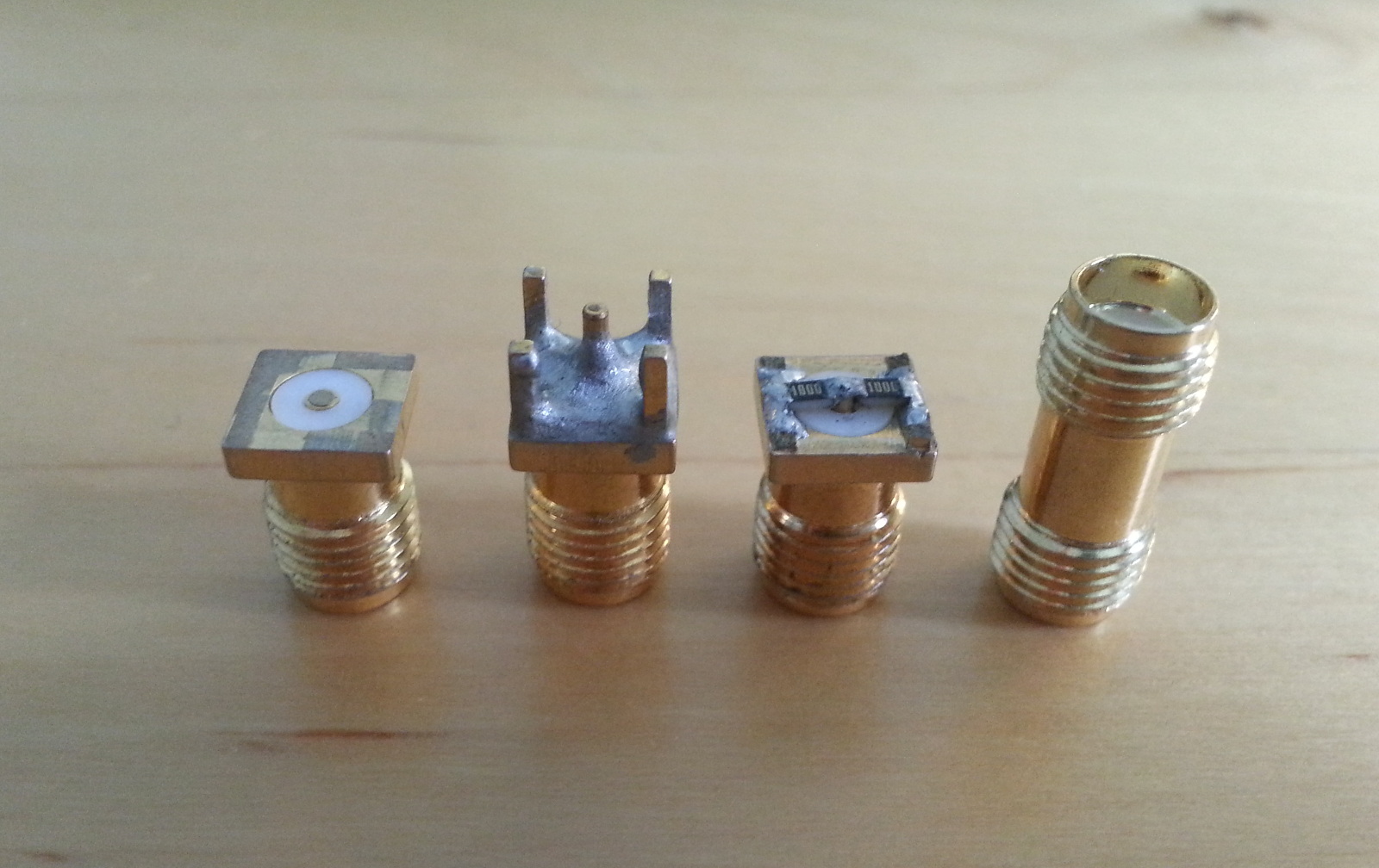
Test board for TRL calibration.
In the above picture is the test board that I made. It has two 50 ohm microstrip lines of different length, one open microstrip line, one microstrip line terminated with 50 ohm resistor and line with 0402 footprint that I populated with a 1 nF capacitor. I'm using this same type of capacitor as a general DC blocking capacitor in my VNA so I'm interested in finding out how it performs at high frequencies.
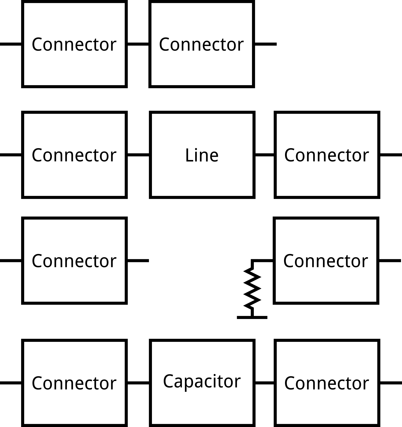
Block diagram of the board.
Using this board and TRL calibration, effect of the connectors can be calibrated out resulting in accurate measurements of the transmission line parameters. Accurate measurement of the capacitor is also obtained, which is useful in a system design. Other 0402 footprint passives can also be populated in place of capacitor to measure them at high frequencies.
If you are not familiar with TRL calibration it is a different method for calibrating a VNA. The normal SOLT calibration uses Short, Open, Load and Thru calibration standard measurements and sets the measurement reference plane to the end of the coaxial connector. Calibration standards need to be known accurately or otherwise there will be errors in the measurements.
TRL calibration uses at least two lines of different lengths and one reflect. No short, open or load standards are needed and unlike standards used with SOLT calibration, lines or reflect don't need to be fully known. Line lengths need to be known, but their electrical behaviour doesn't need to be known accurately. Phase of the reflection coefficient of reflect standard needs to be known within +- 90 degree accuracy. Real reflection coefficient and propagation constant of the transmission lines will be solved during the calibration.
After the TRL calibration reference plane is placed after the SMA connectors on the board. The exact reference plane location is in the middle of the shortest line. For example the capacitor test structure on the board would include the SMA connectors if measured using the SOLT calibration, but with TRL calibration the reference planes are right next to the capacitor pads.
There are few limitations on the TRL calibration:
- Length difference between the lines should ideally be a quarter wavelength. If the measured phase is a multiple of 180 degrees, the resulting system of equation is singular and calibration fails. This results in a limited bandwidth for the calibration but it can be extended by using multiple lines with different lengths.
- Reference impedance of the calibration is the characteristic impedance of the transmission lines and not 50 or 75 ohms as is usual. The measured S-parameters are referenced to this possibly frequency dependent and complex impedance. If the characteristic impedance is not known accurately, the measured results might not be very useful.
Propagation constant
Propagation constant of the transmission line characterizes how phase and amplitude of a wave traveling in a transmission line varies as a function of distance. During the TRL calibration propagation constant is solved and it is one of the outputs of the calibration. Propagation constant varies significantly as a function of frequency and thus can't be really called a constant but that is the established term.
S21 coefficient of a transmission line with length \(l\) can be calculated using propagation constant as: \(S_{21} = e^{-\gamma l}\), where \(\gamma = \alpha + j \beta\) is the propagation constant.
Real part \(\alpha\) of the propagation constant causes loss and imaginary part \(\beta\) causes phase shift. Units of \(\alpha\) are in Nepers/meter, which can be converter to more practical units of dB/m with equation \(20\log_{10}(e)\alpha\). \(\beta\) includes the frequency dependence and looks like a very steep straight line when plotted as is. It can be normalized by dividing by \(2\pi f\), but I think that effective permittivity of the transmission line is a more useful quantity.
Effective permittivity of the transmission line is related to the speed of electromagnetic wave on the transmission line via equation: \(v = \frac{c}{\sqrt{\epsilon_{\text{eff}}}}\), where \(c\) is the speed of light. Wavelength of the electromagnetic wave in a transmission line can be calculated using effective permittivity with: \(\lambda = \frac{v}{f} = \frac{c}{f\sqrt{\epsilon_{\text{eff}}}}\). Since many RF circuits need transmission lines with accurately known length in wavelengths, knowing the effective permittivity accurately is very useful.
Effective permittivity of the transmission line depends on the permittivities of the surrounding materials. With stripline or coaxial cable where the signal conductor is completely surrounded by one material the effective permittivity of the transmission line is equal to the permittivity of the surrounding material. If the TRL calibration would be done for a stripline, the effective permittivity calculated from the solved propagation constant would directly give the permittivity of the material. With microstrip some of the field travels also on the air and the effective permittivity is somewhere between permittivities of substrate material and air. The exact value depends on the line geometry.
Effective permittivity can be calculated from the propagation constant with:
Measurements
All of the following measurements are done using the second version of my homemade VNA.
Unknown thru
Before doing the TRL calibration let's first do a regular calibration to the SMA connectors to see what the S-parameters look like with the SMA connectors.
I'm using scikit-rf Python library for doing the calibration. In the library there are several possible calibration methods to choose from. There is ordinary SOLT that most of the commercial VNAs have builtin, but also several more advanced calibration routines. This time I'm using UnknownThru calibration, because I know the short, open and match standards I'm using well because I have measured them with a commercial VNA, but I don't have a measurement of the through standard. Unknown thru calibration doesn't requires knowledge of the thru standard S-parameters so it is a good calibration to use in this case.
Below is the code for doing UnknownThru calibration:
1 2 3 4 5 6 7 8 9 10 11 12 13 14 15 16 17 18 19 20 21 22 23 24 25 26 27 28 29 30 31 32 33 34 35 36 37 38 39 40 41 42 43 44 45 46 47 48 | |
The measured networks follow the std1-std2 naming rule, where std1 is the standard connected to port 1 and std2 on port 2. Measurements of open, short and load are needed on the both ports. Standards are usually measured as one port on both ports, but in this case standards are connected to both ports and they are measured as a two port. Through also needs to be measured, but with this calibration real through S-parameters don't need to be known. Through can even be a line on the board being measured or any other transmissive circuit that has S21 equal to S12.
Switch terms are needed to account for reflection coefficient of the port switch inside the VNA that causes different termination depending on the measurement direction. They are measured with the ports connected together using any transmissive standard. They can't be calculated from the S-parameters and instead raw receiver measurements are required. It's not an issue with my homemade VNA since accessing the raw receiver outputs is easy, but it can be tricky with some older VNAs. They can also be extracted from SOLT measurements if the receiver measurements are not possible.
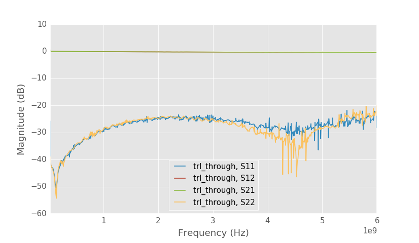
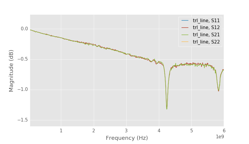
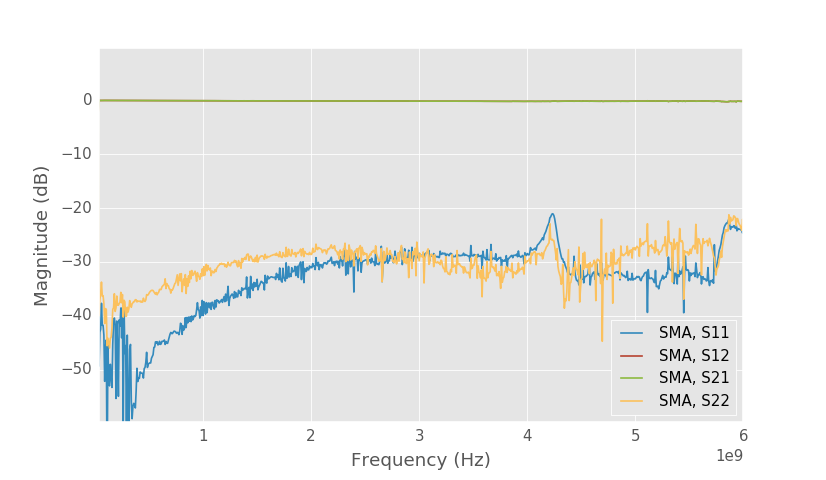
Short line calibrated to SMA connectors.
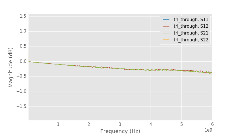
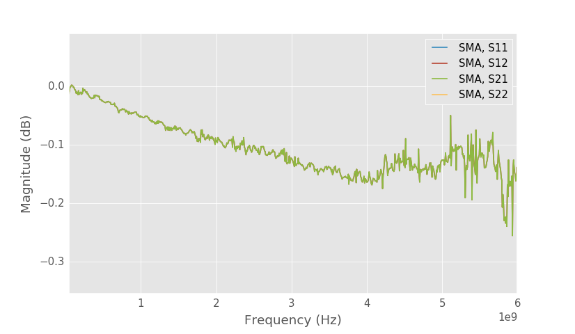
Close up to S21 of short line.
Above is the shortest 5mm long line on the board calibrated to the SMA connectors. It is matched quite well which suggest that the SMA connector matching is also good and that the line is not at least very far off from 50 ohms. Loss is smaller than 0.5 dB even at 6 GHz.
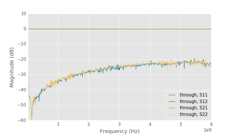
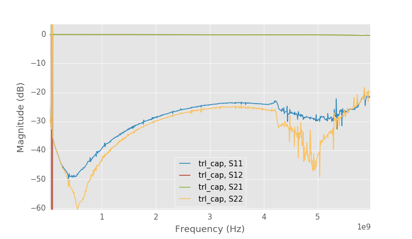
Solved SMA through S-parameters.
Close up to S21 of SMA through.
Above are the solved S-parameters of the SMA through (right side on this picture) that I used for the calibration. Loss is okay, but matching is not spectacular. I guess the through is not exactly 50 ohms. Same results are obtained if the line on the board is used as a through in the calibration.
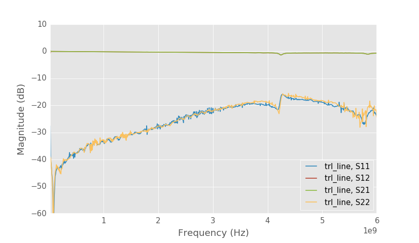
Long line calibrated to SMA connectors.
Close up to S21 of the long line.
Longer 18mm line however isn't performing as well as the shorter one. There are resonances at 4.2 and 5.8 GHz causing increased losses. I measured also another identical board and it has the same resonances. I'm not exactly sure why it happens and I haven't investigated it much yet. Maybe the bottom ground plane works as an antenna? Board has 4 layers and the bottom three layers have a ground plane. The two bottom ground planes are connected to the microstrip ground plane only near the SMA connectors and it is possible that the bottom ground plane is resonating.
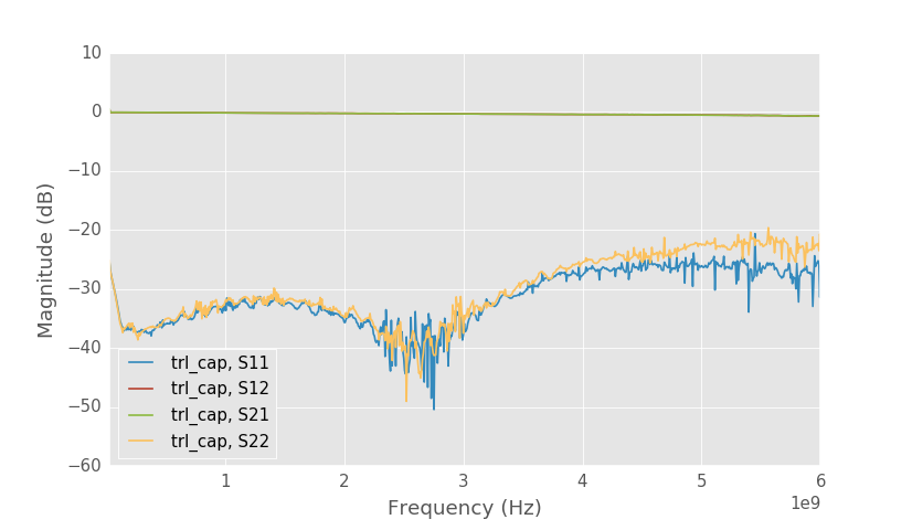
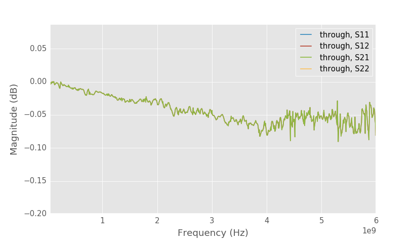
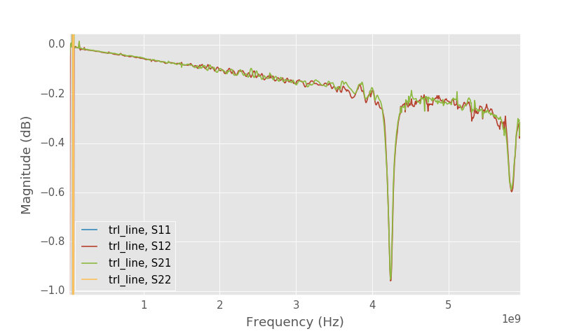
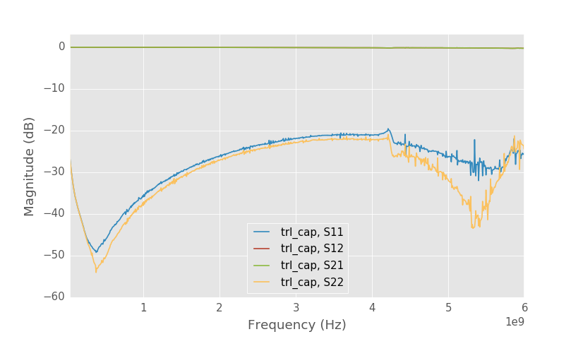
Series capacitor test structure calibrated to SMA connectors.
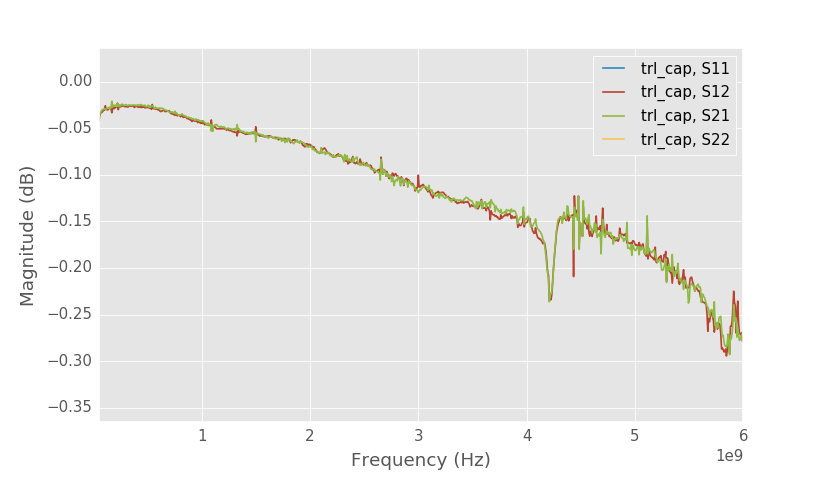
Close up to S21 of the capacitor.
Capacitor test structure doesn't have resonance at 4.2 GHz, but maybe there is a small resonance at 5.8 GHz? Compared to the through line, capacitor test structure has little higher losses as is expected.
TRL
There are three different TRL calibrations in the scikit-rf: Ordinary TRL calibration (TRL), Least squares multiline TRL (MultilineTRL) and NIST Multiline TRL (NISTMultilineTRL).
MultilineTRL is just an alias of TRL, but difference between the TRL and NISTMultilineTRL calibrations is that they behave differently when using multiple lines. Ordinary least squares TRL uses the same system of equations with multiple lines as with just one, but solves it with least squares. It is simple to implement but doesn't avoid singularities if any pair of lines has phase difference that is multiple of 180 degrees. NIST multiline TRL combines the lines more intelligently avoiding the singularities as long as there is one pair of lines that has non-singular phase difference. It allows very wideband calibration even with just a few lines if their lengths are chosen correctly.
In this simple case with one through and one line there shouldn't be difference in the accuracy but I'm using NISTMultilineTRL because it has few features that the TRL class doesn't have.
Below is the code for calibrating the uncorrected measurements:
1 2 3 4 5 6 7 8 9 10 11 12 13 14 15 16 17 18 19 20 21 22 23 24 25 26 27 28 29 30 31 32 | |
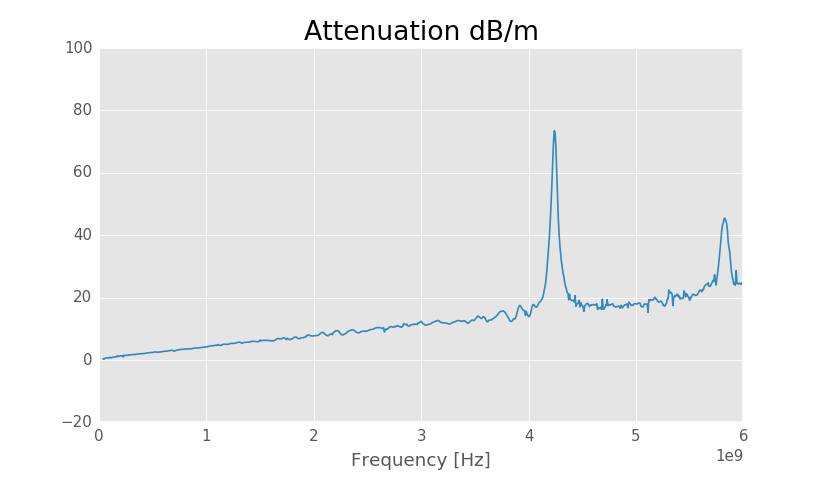
13 mm long line TRL calibration.
The 13 mm long line still has the resonance after the calibration. The resonance will also be visible in all the other measurements since the line with resonance is used in calculating the calibration error coefficients. S11 and S22 are perfect because reference impedance of the TRL calibration is equal to the characteristic impedance of the lines.
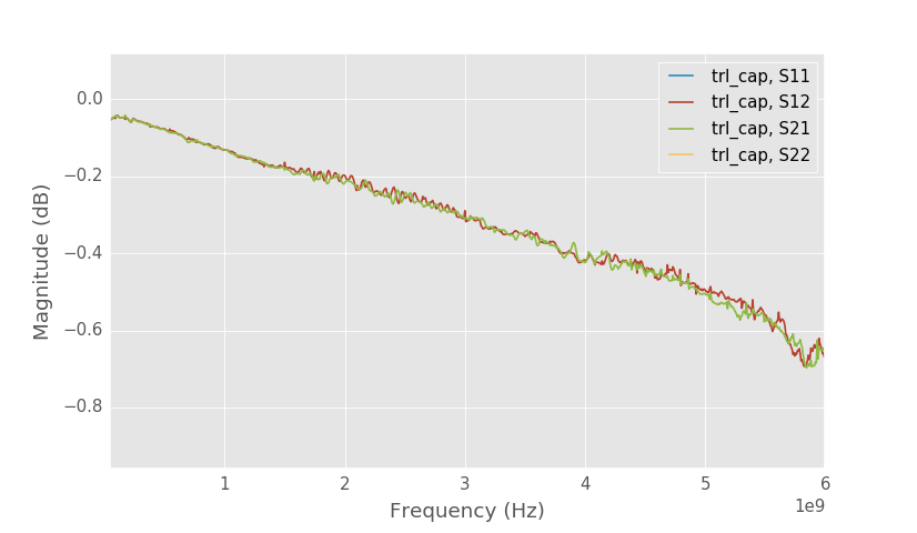
Series capacitor test structure calibrated with TRL.
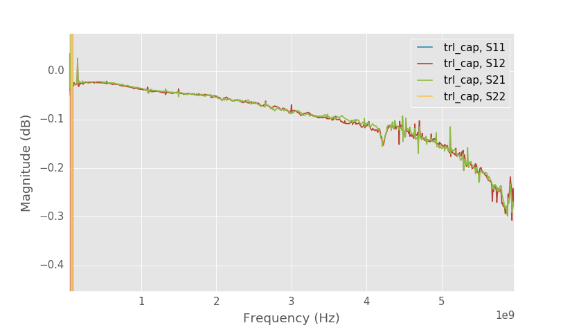
Series capacitor S21 detail.
Above is the capacitor test structure this time calibrated with TRL. With the unknown thru calibration S21 of the capacitor was -0.4 dB at 4 GHz, but with TRL calibration the S21 is only -0.1 dB as the connector losses are calibrated out.
Self resonance frequency of this capacitor is 380 MHz. Equivalent series resistance (ESR) of the capacitor and pads can be determined from the loss at this frequency. Since at self resonance frequency inductive and capacitive reactances cancel out, the capacitor looks like a small valued resistor. S21 of a series resistor can be solved as: \(S_{21} = 2Z_0/(2Z_0+ R)\). S21 of the capacitor is 0.022 dB dB at 380 MHz, giving a series resistance of 0.26 Ω assuming 50 ohm reference impedance. But the reference impedance in this measurement is really the characteristic impedance of the lines. It is probably close to 50 ohms, but characteristic impedance needs to be determined more accurately if a more accurate estimate of ESR is needed.
The solved effective permittivity and line attenuation can be plotted with:
1 2 3 4 5 6 7 8 9 | |
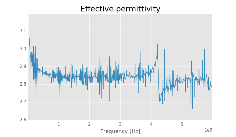
Solved effective permittivity.
Solved line attenuation.
The resonance at 4.2 GHz affects both effective permittivity and attenuation, but below 4 GHz both should be correct. Effective permittivity is quite noisy, but it appears to be around 2.84 at high frequencies and more at lower frequencies.
Line attenuation is around 4.3 dB/m at 1 GHz and 11.6 dB/m at 3 GHz. Using a calculator the theoretical values are 4.9 dB/m at 1 GHz and 11.9 dB/m at 3 GHz.
Accuracy of the calibration can be estimated using the normalized standard deviation plot. It is normalized such that when one through and one line calibration is the most accurate, the phase difference is 90 degrees, the normalized standard deviation is one. When the phase difference goes further from 90 degrees accuracy decreases and the normalized standard deviation increases.
1 2 3 4 | |
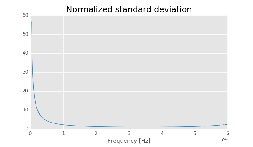
Normalized standard deviation.
As a rule of thumb phase difference between through and line should be between 20 and 160 degrees for an accurate calibration. In the normalized standard deviation plot this corresponds to about three. From the above plot it is clear that at around below 500 MHz the accuracy is much worse than this. To improve the accuracy a longer line that is 90 degrees at low frequencies should be added.
Characteristic impedance
Transmission line lumped element model. Source: Wikipedia
Transmission line can be modeled using sections of lumped elements. Each section represents a short section of transmission line. One section has series resistor and inductor and parallel capacitor and conductance.
Using the lumped section model propagation constant of the transmission line can be defined as:
and characteristic impedance as:
or written using the propagation constant:
Typically conductance (G) of the transmission line is very close to zero if the substrate is not conductive and it can be approximated to be zero. Because propagation constant is solved during the TRL calibration characteristic impedance of the transmission line can be determined if the capacitance per length of the transmission line is known.
C could be measured directly, but it is hard to measure accurately since capacitance of a typical transmission line is very low. Here is a good paper of the possible methods for measuring it.
Measuring characteristic impedance
There are several ways to measure the characteristic impedance of the microstrip lines. The first most simple way would probably be trying to curve fit to the measured lines, but the problem is that we can't fit to the TRL calibrated measurements because TRL calibration's reference impedance is the characteristic impedance of the lines that we want to measure. Fitting to the measurements corrected to the SMA connectors is possible, but accuracy is limited by the matching of the connectors.
Better method without extra measurements is to first calibrate measurements to the SMA connector for example with unknown thru calibration and then do TRL calibration as a second level calibration. Now the TRL calibration error terms represent the S-parameters of the circuit between the reference planes of the calibrations. Unknown thru reference plane was at the SMA connectors and TRL calibrations reference plane is after the SMA connector on the PCB, thus the error terms of the TRL calibration are the S-parameters of the connector. Port impedances of the error terms are 50 ohm from the unknown thru and characteristic impedance of the line on the TRL side. If the SMA connector is short and well matched then the error terms only include the impedance change. Modeling the error terms as an ideal impedance transformer the TRL reference impedance can be solved. There are even enough degrees of freedoms to add a shunt capacitance to the model and still solve the characteristic impedance. For overview of this method see this paper.
We can get the error parameters of the calibration as follows from the calibration:
1 2 3 4 5 6 7 8 | |
VNA calibration can't solve for both S21 and S12 of the error network and instead only the product S12*S21 is solved, which is called reflection tracking. For passive circuit S12 = S21 and we can take a square root of the reflection tracking to solve for S12 and S21. Taking square root leaves 180 degree phase ambiquity, but that is not important when only looking a the magnitudes. Directivity is S11 and source match is the S22.
SMA connector S-parameters from the error terms.
Above is the plot of the S-parameters of the connector from the error terms. Port 1 is the connector side and port 2 is the board side. Port 1 reference impedance is the reference impedance of the unknown thru calibration which is 50 ohms in this case. Port 2 reference impedance is the TRL calibration reference impedance which is the characteristic impedance of the lines that we don't know. At low frequencies we would expect the connector to be matched well, but S11 is only -22 dB suggesting that characteristic impedance of the line is not 50 ohms.
Using scikit-rf we can solve the characteristic impedance with the following code:
1 2 3 4 5 6 7 8 9 10 11 12 13 14 15 16 17 18 19 | |
Characteristic impedance solved from the error terms.
The method is only going to be accurate at low frequencies and in the above plot we can see that the estimated characteristic impedance of the lines is around 57 ohms. Accuracy is not very good and issue with low frequency measurements is that characteristic impedance increases as the frequency decreases. Reason for the increase can be found from the lumped element model characteristic impedance definition:
As \(\omega \rightarrow 0\), \(Z_0 = \sqrt{R/G}\). \(G\) is usually much smaller than \(R\) and \(Z_0\) approaches a large value. At high enough frequencies \(Z_0 \approx \sqrt{L/C}\), which is constant.
Better estimate for the characteristic impedance can be obtained by solving for the capacitance per unit length and using the solved propagation constant from the TRL calibration to estimate the characteristic impedance. This assumes that \(G \approx 0\), which should be true when substrate is not conductive.
1 2 3 4 5 6 7 | |
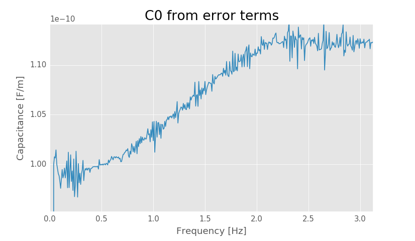
Solved capacitance per unit length.
At low frequencies the capacitance per unit length is about 99 pF/m, but the obtained value is not very accurate because accuracy of the calibration is poor at low frequencies.
Assuming that the capacitance per unit length doesn't vary as a function of frequency, we can use the capacitance solved at low frequencies for solving the characteristic impedance over the whole frequency range. This is usually good approximation to make as long as the relative permittivity of the substrate doesn't vary much as a function of frequency.
1 2 3 4 5 6 7 | |
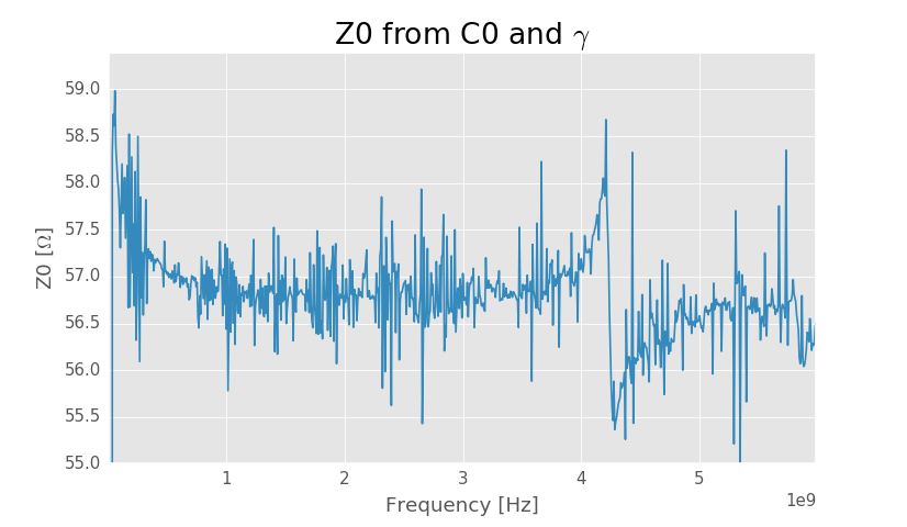
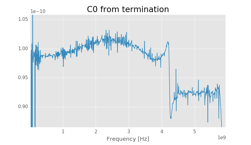
Characteristic impedance from C0 and propagation constant.
The trace is quite noisy and the resonance around 4.2 GHz in the line affects the propagation constant solution causing also the characteristic impedance to be solved incorrectly, but below 4 GHz the solution should be correct. At very low frequencies it can be seen that the characteristic impedance rises as is expected and after 1 GHz it is practically constant. From the plot characteristic impedance of the lines can be estimated to be about 56.7 Ω.
Second method
The previous method assumed that the SMA connector was well matched. A better method that doesn't assume can be used if line there is a terminated line on the board.
At low frequencies parasitics of the termination can be assumed to be low and impedance of the termination is the same as its DC resistance that can be measured very accurately with a multimeter. When the termination is measured with a VNA the expected reflection coefficient is:
This equation can be solved for \(Z_0\), but it is again better to instead solve for capacitance per unit length because \(Z_0\) is not constant at low frequencies.
1 2 3 4 5 6 7 8 9 10 11 12 13 14 15 16 17 18 19 20 21 | |
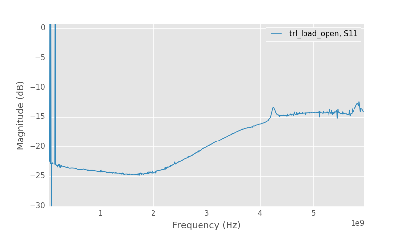
Measured S11 of the termination
Above are the TRL calibrated S-parameters of the termination. At low frequencies the S11 should be very low if \(Z_0=R_{\text{load}}\), but the measured S11 is only -22 dB.
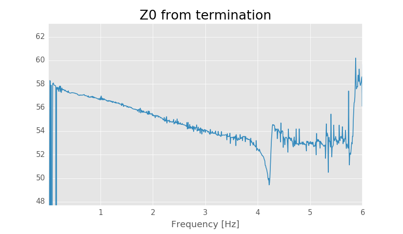
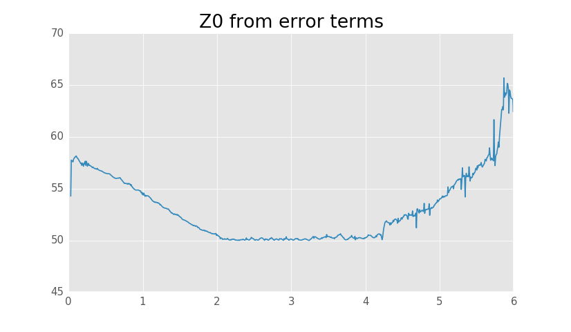
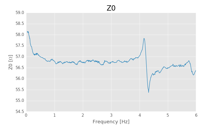
Solved Z0 using termination.
Solved capacitance using termination.
Solved Z0 seems to be around 57 Ω agreeing with the first method. Solved capacitance per unit length is about 98.8 pF/m, when previous method gave 99 pF/m. Now that we have gotten the same characteristic impedance using two methods we should be pretty confident in the result.
Renormalized TRL calibration
Finally the reference impedance of the TRL calibration be renormalized to 50 ohms by giving the capacitance per unit length to the calibration routine:
1 2 3 4 5 6 7 8 9 10 11 12 13 14 15 16 17 18 19 20 | |
Characteristic impedance of the transmission lines. Smoothed using Savitzky Golay filter.
The resonance at 4.2 GHz gives incorrect results around that frequency, but the characteristic impedance can be expected to be constant at high frequencies. Reading from the plot the characteristic impedance seems to be around 56.7 Ω.
The line was supposed to be 50 ohms, but characteristic impedance seems to be over 10% bigger than that, so where's the problems?
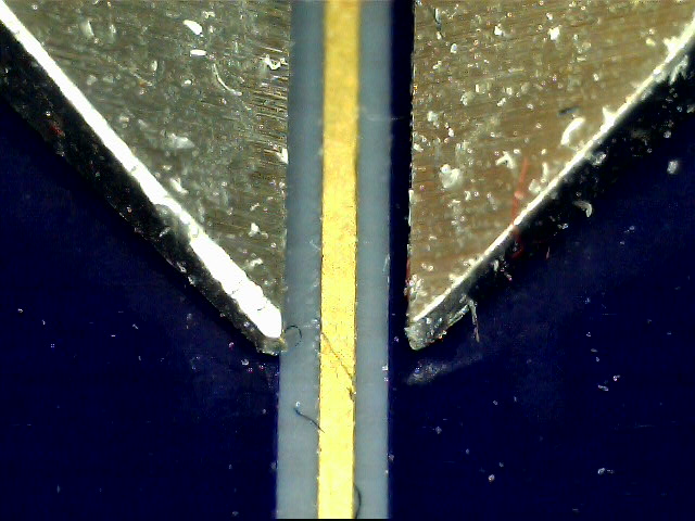
Photo of the line with calibers for scale.
The first thing to check is that the manufactured dimensions of the line match the designed dimensions. In the picture is the microstrip line with calibers set to 1.00 mm for scale. In the image distance between the caliber jaws is 118 pixels, while line is 32 pixels wide. Converting this to mm gives line width of about 0.27 mm. The designed width was 0.34 mm so the manufactured line is thinner, which raises the characteristic impedance. Inputting the measured width to microstrip characteristic impedance calculator with nominal 35 µm trace thickness, 170 µm substrate height and substrate dielectric constant of 3.66 give characteristic impedance of 57.0 ohms.
The observed increase in the characteristic impedance can be fully explained by overetching of the lines. Overetching is about 35 µm, which is not bad considering the price of the PCBs. I have seen bigger overetching on much more expensive PCBs.
Termination S11.
Above is S11 of the termination with renormalized calibration. Now the low frequency reflection coefficient is small as expected. At high frequencies the reflection coefficient is not so good, but this is an issue with the termination and not measurement.
SMA connector S-parameters.
Plotting the solved SMA connector S-parameters from the error terms now gives the true 50 ohm normalized S-parameters. This time the connector matching looks much better. S11 and S22 are below -25 dB up to 4 GHz.
SMA connector S21.
Loss of the SMA connector is also very small.
Capacitor S-parameters.
Capacitor S-parameters don't look that different from before.
Capacitor S21.
At self-resonance frequency S21 is about 0.025 dB, when previously it was 0.022 dB. This gives ESR of 0.29 Ω, when without renormalizing it was estimated to be 0.26 Ω. Error is not very big in this case.
Part number of this capacitor is GRM155R71H102KA01J and Murata makes its S-parameter measurements available on their website.
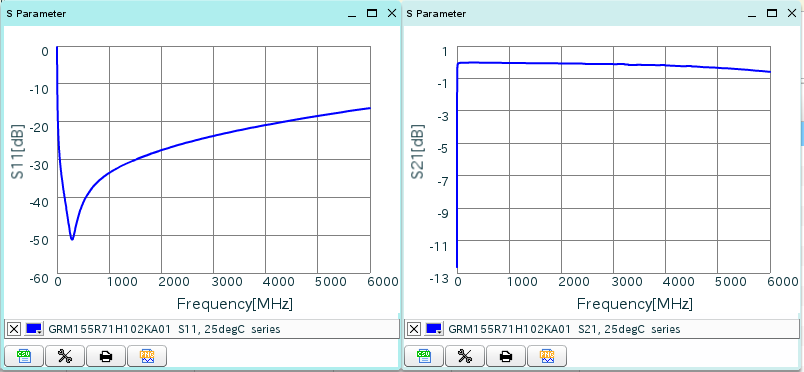
Capacitor S-parameters from manufacturer.
My measurements include the PCB pads which cause some extra capacitance at high frequencies, but S-parameters measured by the manufacturer look very similar to what I measured. The manufacturer has measured the ESR to be 0.277 Ω which agrees really well with my measurement of 0.29 Ω.
Conclusion
Even though my VNA is much less accurate than commercial VNAs it is accurate enough for many useful measurements. I tried the same measurement also with the first version of the VNA and due to the much worse isolation the results were unusable.
The board had unfortunate resonance at 4.2 GHz, which I think comes from the poor grounding of the multiple ground planes. I think I'll need to order a new PCB with better grounding.