Introduction
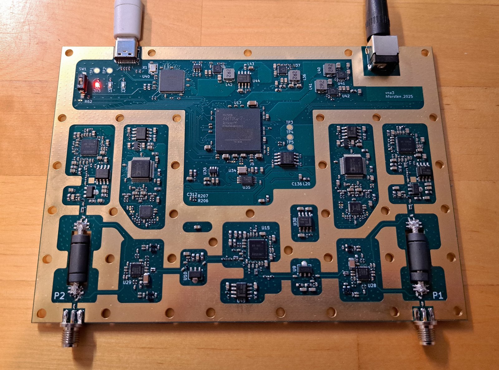
VNA PCB.
Vector network analyzer is a device used to measure scattering parameters of electrical circuits operating at high frequencies. S-parameters tell how much a circuit reflects power back to the source and how much it attenuates or amplifies it to the other ports. Working with S-parameters is an essential part of designing any electronics operating at GHz frequencies.
These devices aren't cheap, especially as the operating frequency increases. High end VNAs that operate at millimeter-wave frequencies can cost several hundred thousand dollars, and even affordable lower-frequency devices are expensive.
My two previous homemade VNAs.
In 2016, I made my first cheap 10 MHz to 6 GHz two-port vector network analyzer. At the time, there were no cheap VNAs available, and I had to design one myself. It was functional but had high leakage between the two ports, causing big measurement inaccuracies, which resulted in unusable accuracy for many measurements. The next year, I designed improved version that had better performance and was actually useful. I have used it since for my own projects, but lately, it has started to feel limiting, and I wanted to either buy or make a better VNA. I would want to have higher maximum frequency, hopefully >10 GHz, better measurement accuracy, and good port-to-port isolation.
nanoVNA (left) and LibreVNA (right).
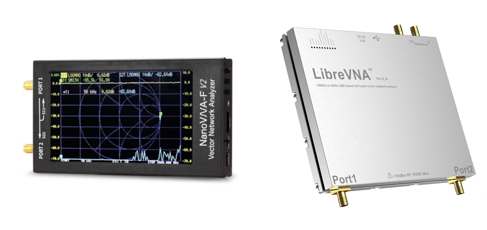
Nowadays, there are many cheap commercial VNAs. The most popular is probably nanoVNA. There are several different versions of it, but they are mostly limited to around 1 - 4 GHz, which is not enough for me. It's also a so-called 1.5-receiver design that can only measure S11 and S21, requiring manually flipping the device being measured to fully measure the two-port S-parameters. It isn't any better than what I already have. There are also several other 1.5-receiver VNAs, some better and some worse, but the 1.5-receiver architecture is too limiting and results in inaccurate measurements to be worth considering.
A step up on that is LibreVNA. It's a 100 kHz to 6 GHz two-port VNA that was partly based on my previous VNA design. It has better performance than my previous 6 GHz VNA, but the performance isn't as good as I would want. There is quite high leakage above 3 GHz that limits the measurement accuracy. Unlike the nanoVNA, it's a proper two-port VNA that can measure two-port S-parameters without manually requiring flipping of the device. However, it's a three-receiver design instead of a better-performing four-receiver design. There is a shared reference receiver before the port switch that is used for measuring the output signal instead of two separate reference receivers for each port. Using advanced calibrations such as TRL, and unknown thru requires a two-port VNA with four receivers. These are very useful as they relax the requirements on how well the calibration kit needs to be known, increasing the measurement accuracy, especially when using a low-cost, inaccurate calibration kit.
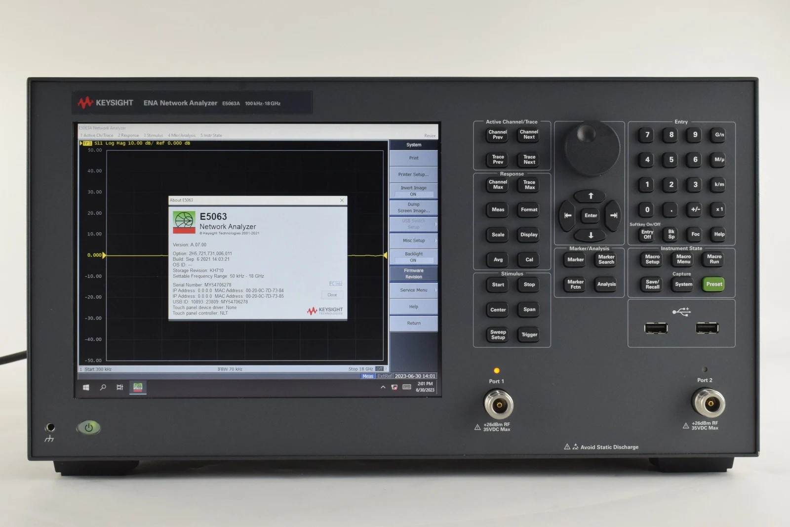
Keysight E5603 VNA. 100 kHz to 18 GHz option has a list price of 53,000 € and this isn't even a high-end model.
There are better performing VNAs that would be perfect for my requirements, such as those from Copper Mountain or Keysight, but even the cheapest >10 GHz VNAs are over ten thousand dollars.
I was unable to find a cheap two-port VNA that would meet my requirements, but after thinking it a bit, I was quite sure that I could make my own VNA that would have better performance than any other cheap VNA currently available, even when factoring in the higher prices at small prototype quantities.
VNA architecture

Generic block diagram of a four receiver VNA.
A typical VNA consists of excitation and local oscillator signal sources. The source is routed through a port switch to one port, with the other port being terminated to 50 ohms. The signal then passes through directional couplers, which sample the incident and reflected waves. These waves are mixed with the local oscillator to convert them to low frequencies that can be sampled with an ADC. These measurements can be used to calculate both the amplitude and phase of the reflected and transmitted waves.
A major issue with this architecture is the port switch. It requires >100 dB isolation over the whole operational bandwidth of the VNA, which is very hard to achieve, requiring that several RF switches in their separate shielded enclosures are put in series. Especially at >10 GHz RF switches, shielded enclosures, and amplifiers can get quite expensive.
Traditionally, designing a wideband RF signal source has also been a challenge. Often requiring multiple mixers, oscillators, filters, and frequency multipliers to achieve high-quality signal over the entire VNA frequency range. However, nowadays there are cheap PLL chips with integrated bank of VCOs that can generate signals over very wide frequency range. For example, LMX2594 is a 10 MHz to 15 GHz RF signal source in a single package that costs $38 at large quantities.

Block diagram of dual-source VNA.
Using integrated phase-locked loop (PLL) ICs for the source signal generation makes it possible to remove the port switch and instead have separate signal sources for each port. This is both cost-effective and simplifies achieving the isolation requirement.
The drawback is that variable attenuator for source power level control and filter bank for filtering the harmonics needs to be duplicated for each port. However, if low adjustable source power range is acceptable, the external variable attenuator can be removed, and the internal power adjustment of the PLL chip can be used instead. The LMX2594 output power can be adjusted by about 10 dB.
Filter bank can also be removed if harmonics are acceptable. Ideally, harmonics shouldn't affect the S-parameter measurements when measuring linear devices. However, in practice there can be some non-linearity in the receiver that causes harmonics to mix to the fundamental frequency. Including the filters would slightly improve the measurement quality.
After looking at the prices of variable attenuators and RF switches at 15 GHz, I decided that I'm fine with the harmonics and low output power adjustment range.
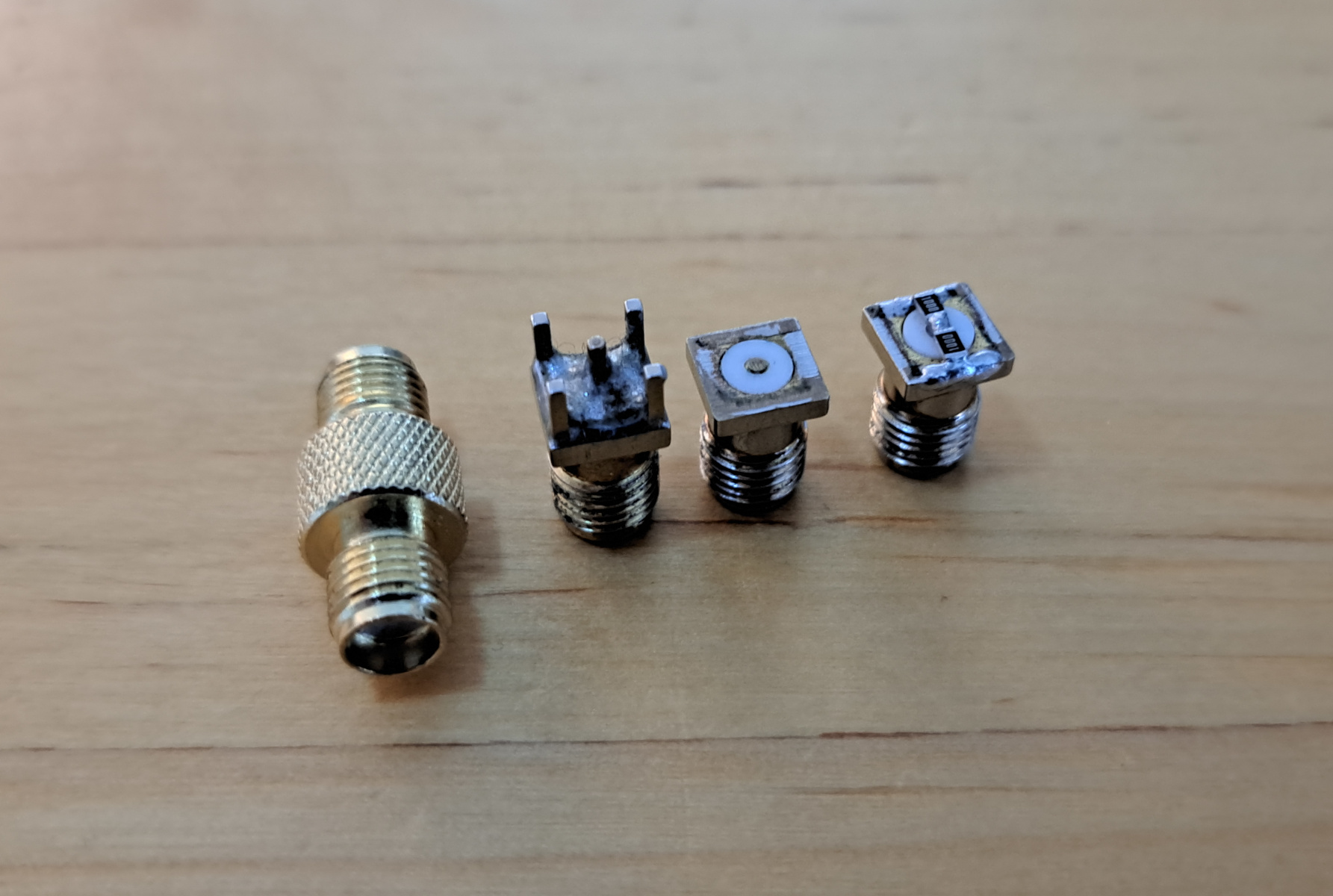
Directional couplers

Directional coupler schematic.
VNA needs directional couplers to sample the incident and reflected waves at both ports. These couplers should also operate from 10 MHz to 15 GHz with good directivity and low loss. The standard directional coupler used in many commercial VNAs is a resistive directional bridge. It requires a balun, which in this case is implemented with a coaxial cable surrounded by ferrite beads to extend its operation to low frequencies.
In my previous VNA, I used a similar directional coupler but it only had one coupled port. I realized that in this application, when two couplers are needed that sample reverse and forward waves, two couplers can be put back-to-back sharing the same coaxial cable balun, which makes it smaller.
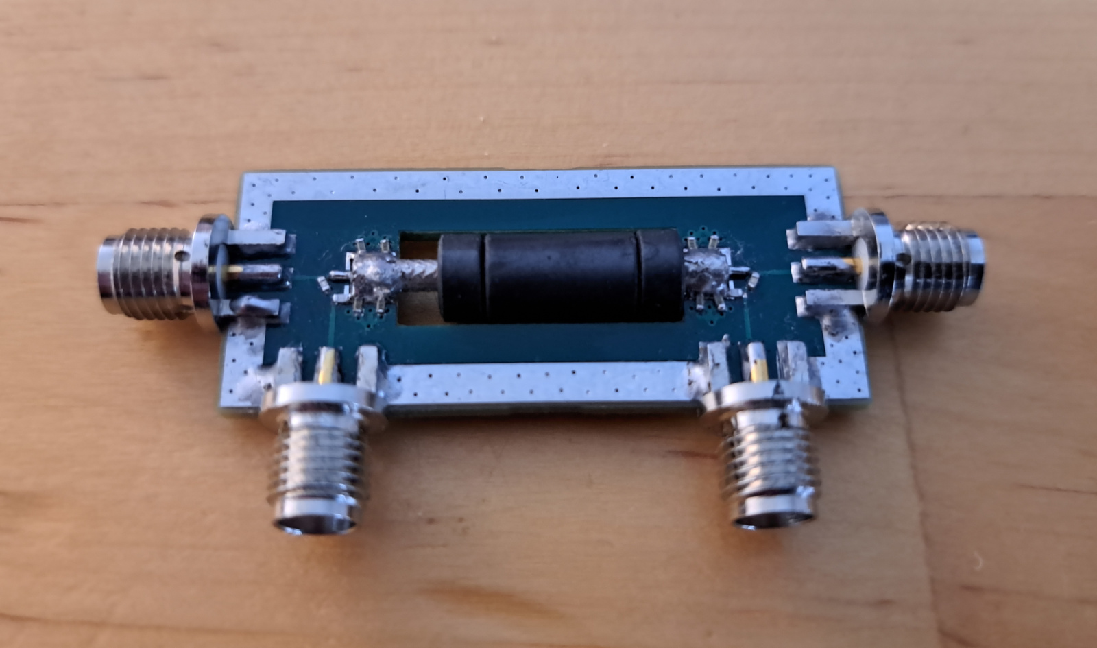
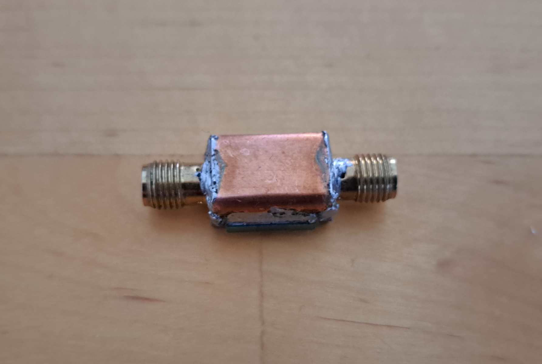
Directional coupler breakout PCB.
I made a breakout PCB of the coupler so I could measure it as its performance is very important for the VNA. PCB material is FR4, which is quite lossy at high frequencies, but proper RF material would be too costly.
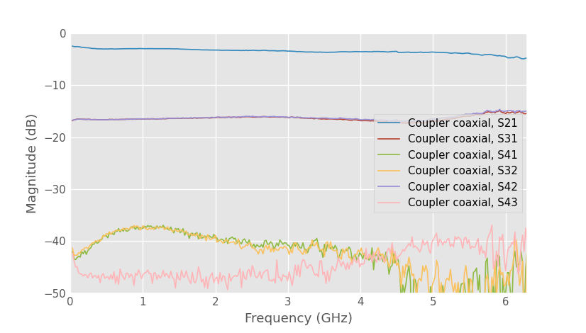
Measured S-parameters of the coupler. Ports 1 and 2 is the thru path, and ports 3 and 4 are coupled ports.
I measured the coupler with my previous 6 GHz VNA, and the performance looks good. It's a four port, but this is not a problem and only requires making multiple measurements. Loss is 3 dB at low frequencies and 5 dB at 6 GHz. Directivity is about 20 dB, which is fine but could probably be improved with slightly tuning the resistor values. Isolation between the coupled ports is acceptable, and there doesn't seem to be issues with sharing the balun.
Receiver
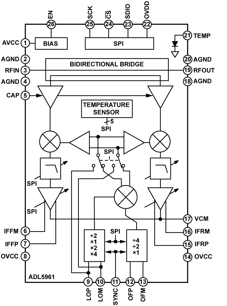
ADL5961 block diagram. This would be an ideal receiver for the VNA if it wasn't for the price. It has integrated directional coupler and even LO frequency dividers and multipliers.
The receiver needs to first down-convert the RF signals from the directional coupler and then sample it with an ADC. Finding a wideband mixer turned out to be problematic. ADL5961 would be an ideal choice as it's rated from 10 MHz to 20 GHz, it's designed for VNA applications, and even includes a directional coupler on the chip. The drawback is that it costs $200 for a single chip, and two of them (one for each port) would cost more than all the other components combined.
The other options are very limited. Many mixers function at high enough frequencies, but almost all of them also have high minimum frequency. I could have two mixers for low and high frequencies that are switched, but it would cost too much. Some mixers could have enough conversion gain at low frequencies even if operated out of spec, but I don't want to test them individually. Another option would have been to make my own mixer with diodes, but this would require a large amount of testing and the resulting circuit would likely be much larger than the small commercial integrated circuits.
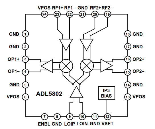
ADL5802 dual channel mixer block diagram.
In the end, I chose to use ADL5802, which is only rated from 100 MHz to 6 GHz. Unfortunately, this limits the performance at high frequencies when everything else would work fine. However, I don't see other cheap options. They main benefit of it is that it's cheap ($12 / piece at high quantities) and it has two mixers in one package, further driving down the cost. The reason I chose to use it is that it does have some performance figures listed at 8 GHz that suggests that it has 5 dB lower conversion gain than at 6 GHz. Even if it doesn't function well above 8 GHz, this should be good enough as I mostly currently work at frequencies under 7 GHz.
ADC

Receiver dynamic range plot (not to-scale).
The dynamic range of the analog-to-digital converter (ADC) is critical because it often limits the receiver's dynamic range. The mixer output can vary from the noise floor (approximately -160 dBm/Hz) to about +10 dBm at maximum input power at the 1 dB compression point. This wide dynamic range exceeds what most ordinary ADCs can handle. The ADC's dynamic range depends on the noise in a single sample and the number of samples averaged. Faster low-bit ADC can be more accurate than slow many-bit ADC when many samples are averaged.
The mixer output frequency should be at least a few hundred kHz to minimize the effects of phase noise and 1/f noise. A higher intermediate frequency (IF) allows for shorter measurement times, as at least few cycles of the IF must be sampled. Some margin should be also left for the ADC's anti-alias filter roll-off. A higher sampling rate also improves spectrum analyzer performance but increases the ADC cost.
The key performance metric for the ADC's dynamic range is noise spectral density (NSD). Many ADCs instead report signal-to-noise ratio (SNR) of a single sample instead. Using the sampling rate, NSD can be calculated as:
\(\text{NSD} = -\text{SNR} - 10\log_{10}(f_s/2)\)
where \(f_s\) is the sample rate. Typically its around -140 to -160 dBFS/Hz (noise floor decibels relative to the ADC full-scale input at 1 Hz bandwidth). In practice this figure tells the FFT noise floor of the ADC output as function of measurement length. For example, with a 0.1-second measurement time and an NSD of -140 dBFs/Hz, the FFT noise floor is -130 dB below the full-scale non-clipping input.
The ADC I chose to use is AD9238 which has 40 MHz maximum sampling frequency and an NSD of -143 dBFs/Hz. Since the ADC's dynamic range is less than dynamic range of the mixer's output dynamic range, either high input causes ADC saturation or the ADC's noise floor is above the mixer's noise floor. In this case it's a bit of both.
With an NSD of -143 dBFs/Hz, if the incident wave power is at -10 dBFs level at the ADC input, the dynamic range for S21 measurement is at most 133 dBFs/Hz since it's calculated as the ratio of port 2 received power divided to port 1 incident power. With a 10 Hz IF bandwidth, the S21 measurement will have a noise floor of -123 dB. If the source power is lower, the incident power decreases, and the S21 noise floor increases.
If the cost is not an issue, better choices are available. For example, the AD9650 (105 MHz version) has an NSD of -160 dBFs/Hz. It would increase the dynamic range by about 17 dB. It's also about ten times more expensive, so the performance doesn't come cheap.
FPGA

FPGA digital signal processing block diagram.
Fast sample rate ADCs need an FPGA to handle the high amount of data they produce. The same FPGA can also handle all the DSP and I/O control functions, avoiding the need for adding a separate microcontroller.
The digital signal processing needed inside the FPGA is deceptively simple. The input signal from each of the four receivers is a signal at a few MHz frequency. It's multiplied with a sin and a cos of the same frequency signal to get a zero frequency I and Q output signals that are summed. At the end of the sampling period, these I and Q accumulated sums are divided by the number of samples summed to get the average value. This is equal to calculating just a single bin of Fourier transform and is the optimal way of calculating magnitude and phase of a signal at a known frequency.
The rest of the logic on the FPGA is timing, switching I/O signals, and communicating with the PC. All of the logic and calibration is implemented on PC as it's much easier to do there.
PCB
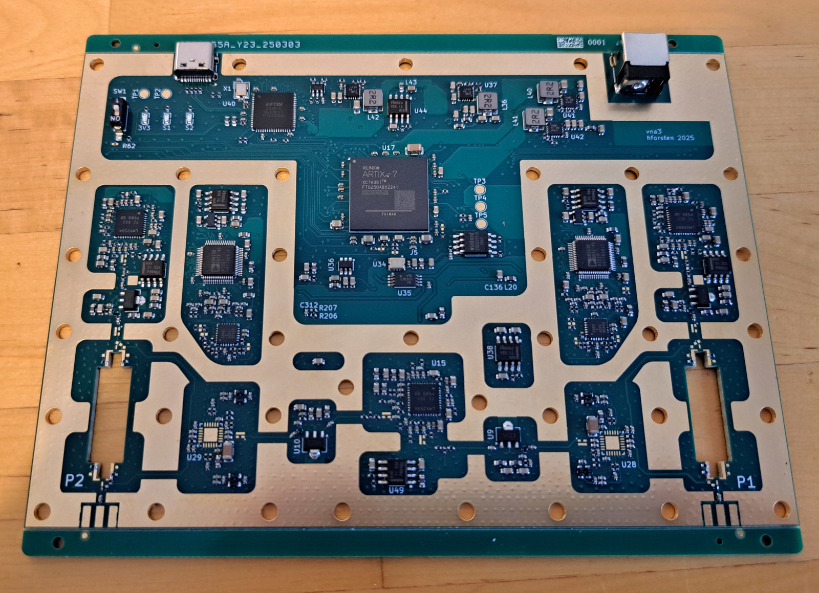
Partially assembled VNA PCB.
PCB has 6-layers and is made from FR4 material. FR4 is fine in this application since distance from signal source to output port is quite short and there aren't any sensitive circuits such as distributed filters that are sensitive substrate material variations.
For good isolation RF enclosure is necessary and it requires mounting holes and contact surfaces on the PCB. Isolation was the biggest issue with my previous VNA and I did everything to make sure that this time the leakage signal will be below the noise floor. Due to the high frequency all the RF signals are routed at the top layer, requiring routed channels in the shield to pass the signal via the different enclosures.
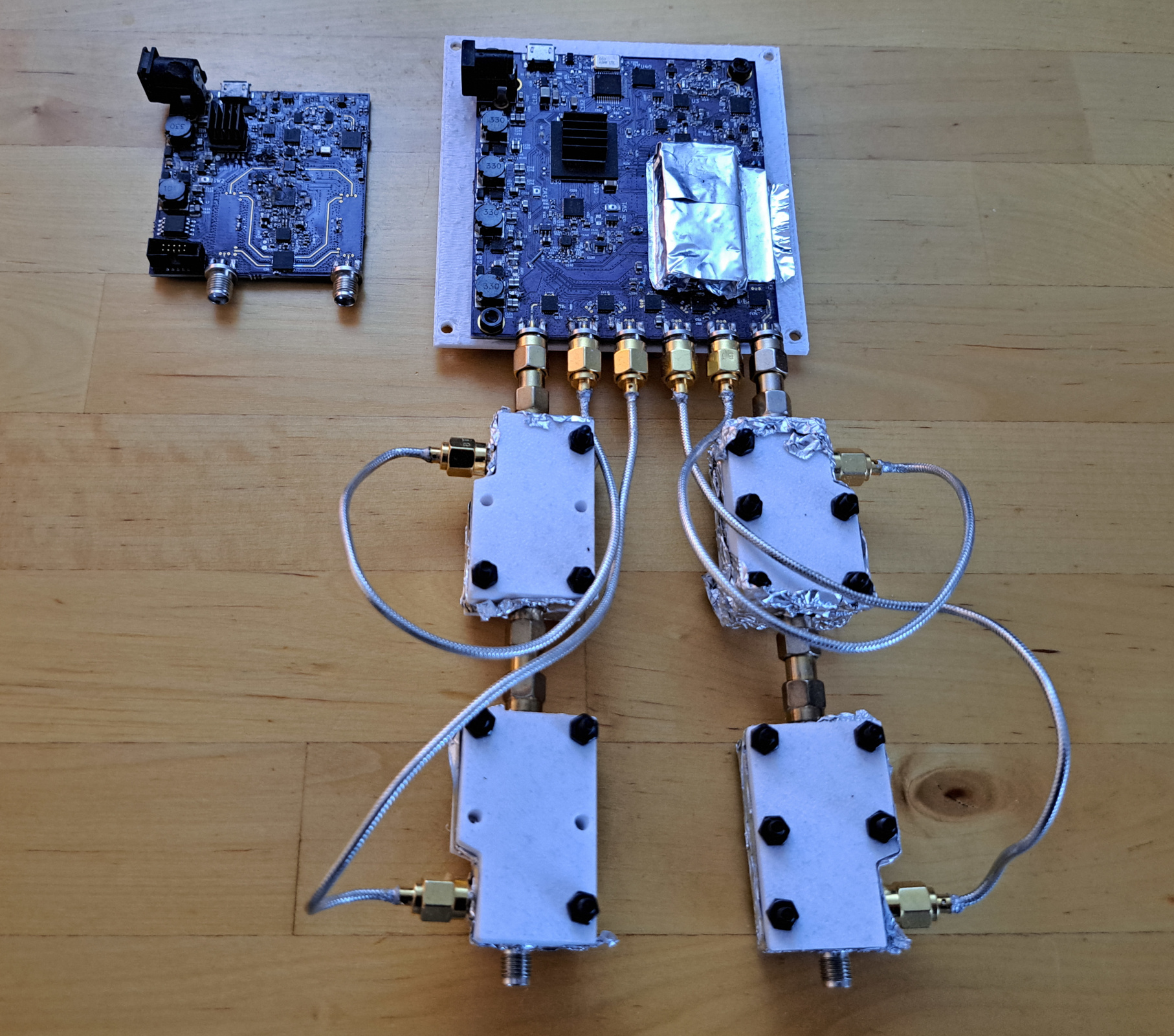
Assembled VNA.
I ordered the PCB assembled but I had to assemble some components such as mixers, SMA connectors, and couplers myself. When considering a large scale production the couplers are especially tricky as they require manually cutting a coaxial cable, inserting ferrite beads into it, and the soldering it to the PCB. In this case it isn't an issue when I just make one PCB for myself, but this would be difficult for mass manufacturing.
CNC machined case
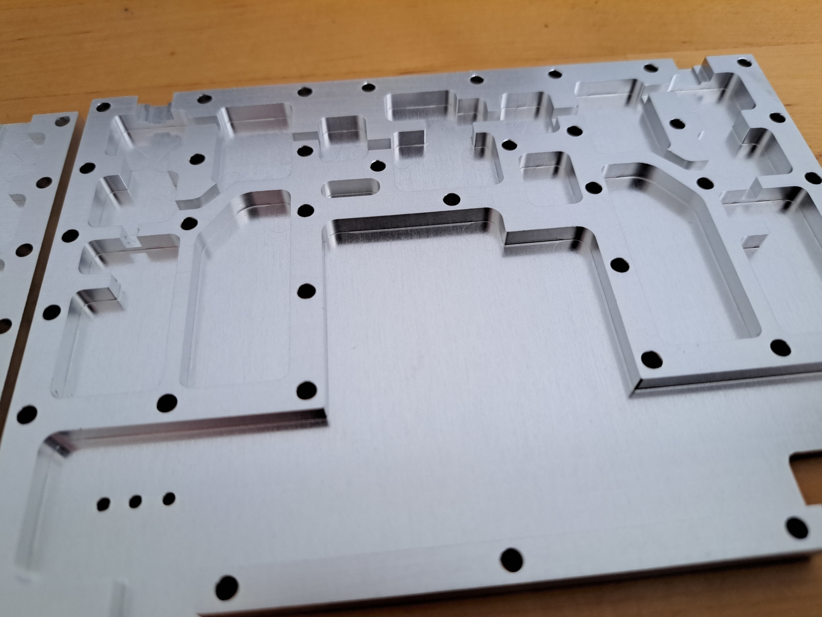
CNC machined case, upper half.
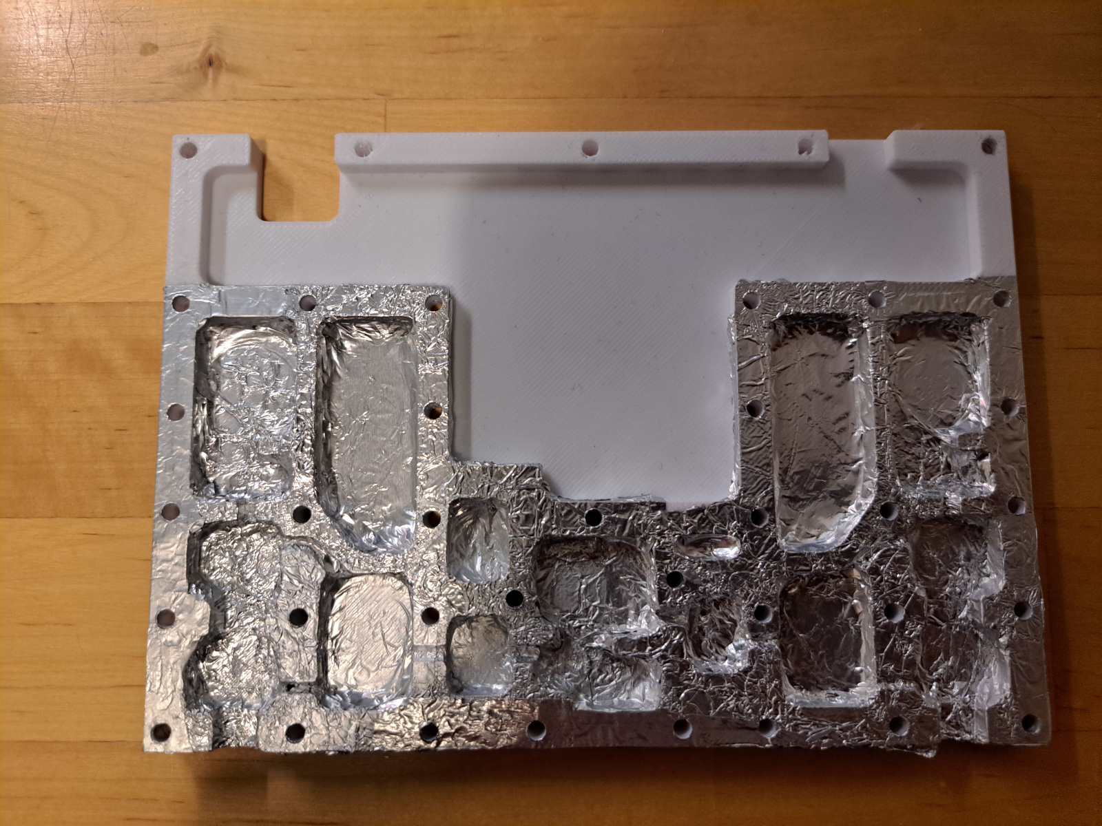
I first made a 3D printed case lined with aluminium foil for testing the electronics and making sure the mechanical design fit the PCB. It had quite good isolation after I figured how to get the aluminium foil lining to be tear free. Stability and thermal properties of the CNC machined case should be much better, so I ordered the same design machined from aluminium.
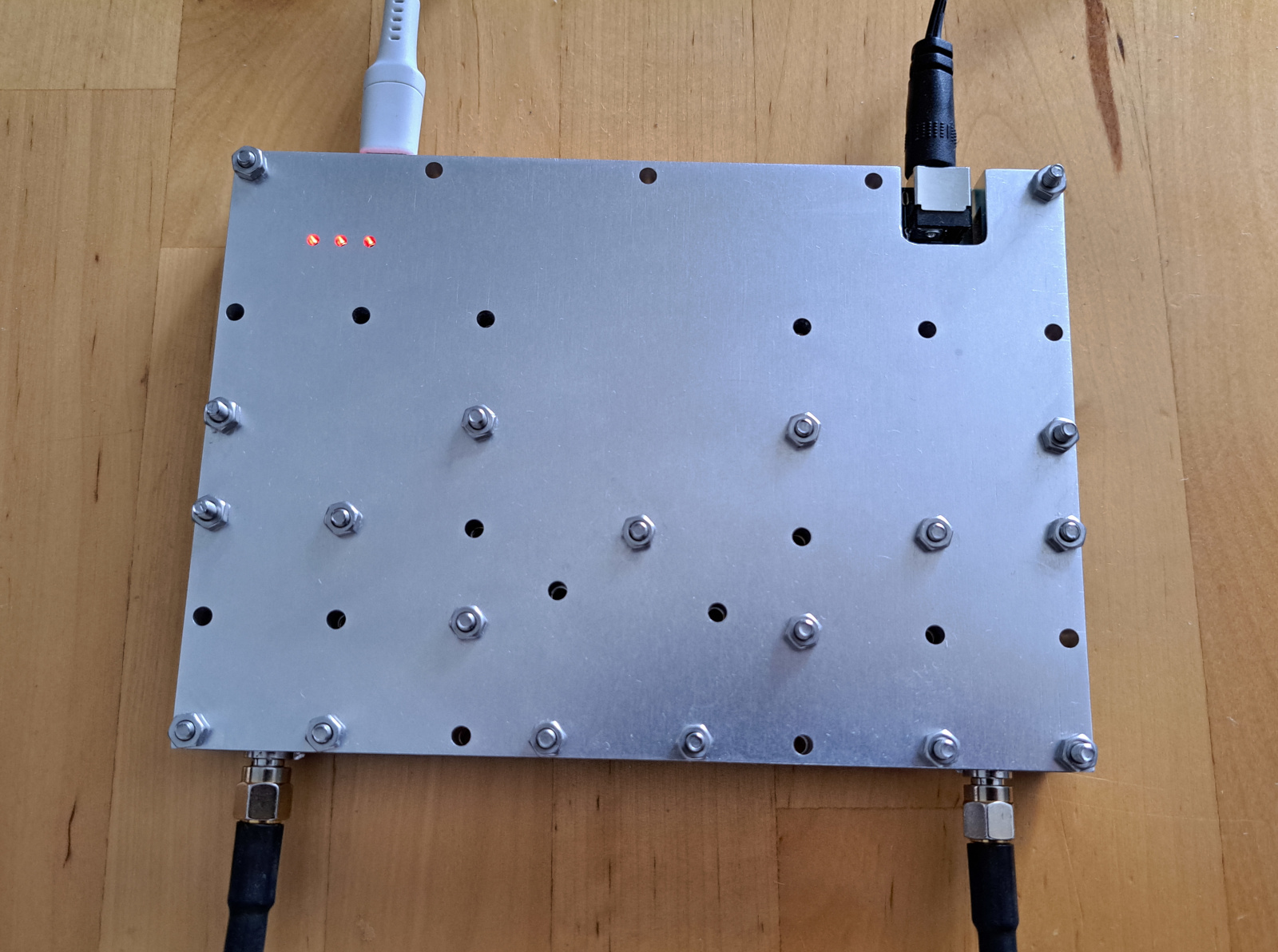
VNA with the aluminium case.
The case consists of upper and lower pieces with the PCB being sandwiched between them. I designed it to be simple so that it can be manufactured on a 3-axis CNC machine in a single pass and without any threads. The cost was $75 for the case, $37 for shipping, and $29 for taxes. Not bad for a fairly large piece of aluminium.
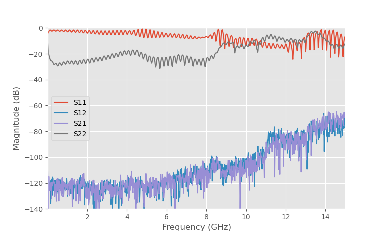
Uncorrected S-parameters with short on port 1 and load on port 2. 200 Hz IF bandwidth.
The leakage with the CNC machined case was surprisingly high when I first assembled it. Uncorrected S21 was higher than -70 dB at 6 GHz. The culprit turned out to be a gap between the edge launch SMA connectors and the aluminum case. The gap between the connector and the case is very small, less than 1 mm, but it works as an antenna just well enough that the coupling to the other port was about -70 dB.
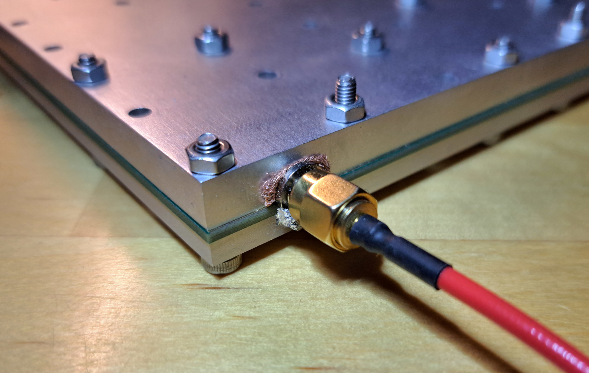
Solder wick and aluminium foil used to seal the gap between the SMA connector and the aluminium case.
I used aluminium foil to plug the gap between the bottom case half and the connector. A small folded up piece of foil placed under the PCB compresses nicely and provides good RF seal. The upper half can't use the same method since it would short the signal conductor. I used instead a small piece of solder wick to seal the upper half gap.
I knew that this connector gap could be an issue when I first designed the VNA, but I decided to go with it because the alternative of using a bulkhead SMA connector (the whole connector goes through the case) was just too much trouble. Bulkhead connectors would need a hole and threads in the case in 90-degree angle from the current machining direction. Bulkhead connectors would also need to be soldered to the PCB when it's mounted in the case, making it inconvenient for prototyping.
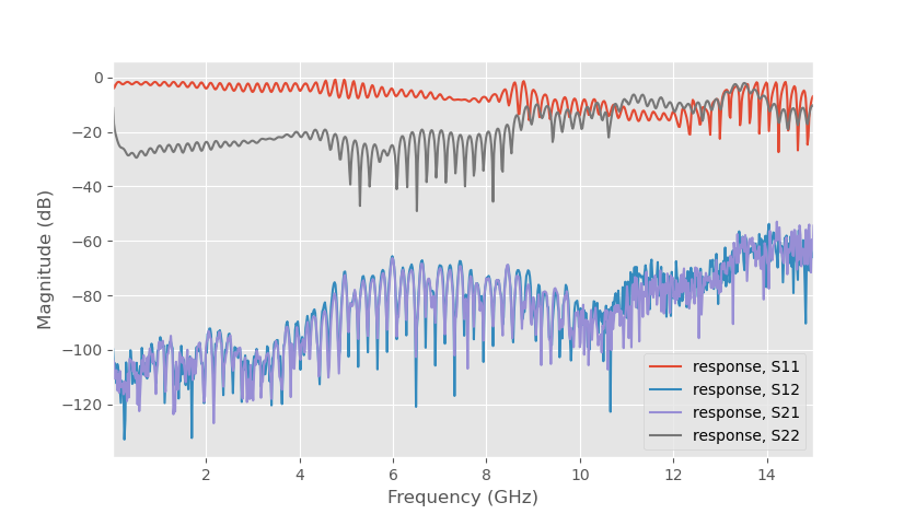
Uncorrected S-parameters with short on port 1 and load on port 2 with EM gasket. 10 Hz IF bandwidth.
After plugging the gap, the isolation is much better and leakage is below the noise floor at all frequencies even with very low 10 Hz IF bandwidth (0.1 s measurement time per frequency point).
The noise floor increases as the source frequency rises. This is because the mixer's conversion gain decreases beyond 6 GHz. The dynamic range is still quite good up to about 10 GHz, but starts to quickly decrease after that. While the dynamic range was 120 dB at low frequencies, it's less than 70 dB at 15 GHz.
Calibrated S-parameters with short circuits on both port 1 and port 2. 10 Hz IF bandwidth.
After the calibration, the dynamic range is slightly lower at high frequencies due to the losses that need to be calibrated out, but the difference isn't large due to directional couplers still working with acceptable performance. While the lower dynamic range at high frequencies might not be good enough for precision measurements, it's still useful for many basic measurements.
Harmonic mixing
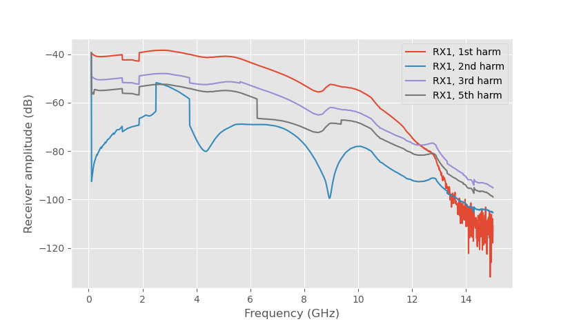
Reference receiver measurement at different LO harmonics (arbitrary scale).
Mixer is rated only up to 6 GHz operation and it has an integrated LO amplifier. At high enough frequencies the LO amplifier's output power isn't high enough to drive the mixer core. If the LO is driven at for example 1/3 of the desired frequency, the fundamental frequency should be high enough to still pass through the integrated LO amplifier and there should also be some harmonic mixing products at the output caused by the third harmonic of the LO.
I swept the source from 0.1 GHz to 15 GHz with LO set to different harmonics. The results of the reference receiver power (arbitrary scale) are shown in the image above. The result is magnitude of the mixer's output, which is proportional to source power coupled into reference receiver and the conversion gain of the mixer, so this measurement doesn't just measure the mixer. As expected, the fundamental frequency results in the highest conversion gain at the mixer's operational range. The IF signal is about 15 dB lower at 10 GHz, which is still acceptable, but above that it starts to drop quickly. The output also becomes very noisy, likely due to LO drive power being too weak. At around 12 GHz, using the LO at 1/3 frequency for 3rd harmonic mixing results in higher output power. Other LO harmonics than 1st or 3rd results in lower conversion gain.
The LMX2594 chip seems to have a 2 dB dip in output power from 1.25 GHz to 1.875 GHz when the output frequency divider value is set to 6. This dip is visible in all traces at that frequency range due to source power being lower. The same effect due to LO source power can also be seen at higher frequencies at different LO harmonics.
Some VNAs use a similar trick with source harmonics to extend the maximum frequency range. For example, to measure S-parameters at 20 GHz, set the source to 10 GHz and use the 2nd harmonic of the signal as the test signal. The LO would be set to (20 GHz + IF frequency)/3 = 6.67 GHz for the LO 3rd harmonic. However, this method can't be used to measure any even slightly non-linear devices, as the non-linearity of the device would cause the harmonics to change due to the strong fundamental signal that is still present. Similarly, the receiver's non-linearity can cause issues. Driving mixer LO with harmonics doesn't suffer from the same issues.
Stability
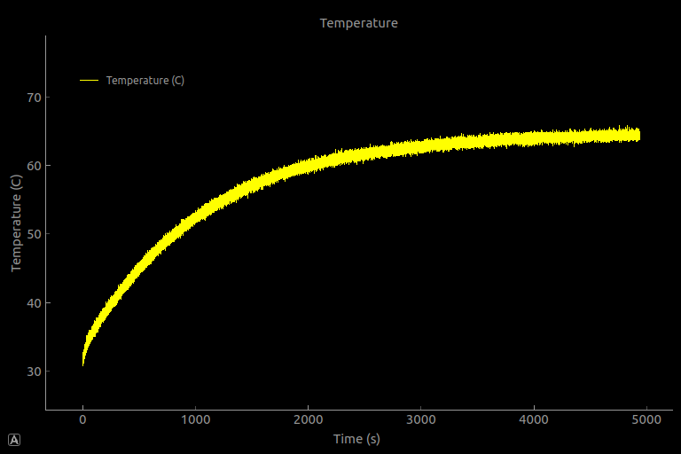
Temperature of the FPGA.
The board does get quite hot, I estimated that it dissipates about 10 W of power. The FPGA's internal temperature sensor indicates a die temperature of 64 C (147 F). The case also gets uncomfortably warm to touch. It takes about 1 hour to reach the equilibrium temperature.
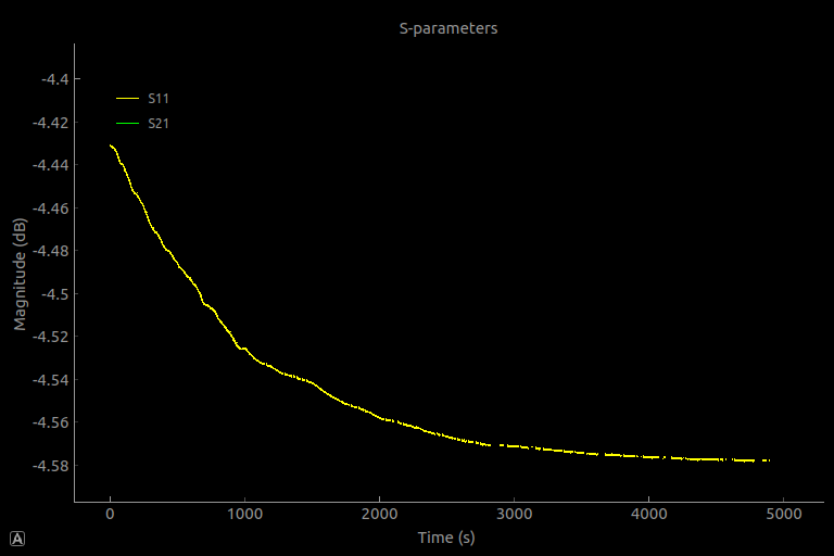
Uncorrected S11 of short at 6 GHz as the VNA warms up.
Temperature has an effect on the measured S-parameters. With a short circuit at port 1, uncorrected S-parameters measured at 6 GHz changed from -4.43 dB at room temperature to -4.58 dB when warm (this includes VNA internal losses and external 0.5 m long SMA cable loss). Source power should drop at high temperatures, but since S11 is a ratio, it should cancel out. Incident and reflected wave mixers are in the same package, well-matched to each other, and at the same temperature, so their conversion gain change should also cancel out. This just leaves the coupler as the likely cause the drift.
One possible reason for thermal drift is that FR4 PCB dielectric constant and loss tangent can have large temperature variation. Copper resistance also increases with the temperature. The loss of coaxial cable is about 7% larger at 60 C than at room temperature, and microstrip lines on the PCB likely have even greater loss increase. Difference between incident and reflected waves is that the incident does not go through the coupler but reflected wave does, so it should be expected that the uncorrected S11 decreases slightly as temperature increases due to increased loss of the coupler. Resistors in the coupler also change slightly with the temperature.
I tried measuring the change in coupler's loss at different temperatures using the coupler breakout board and heating it up with a hot air tool. I don't have a thermal chamber at home, so the measurement accuracy is low but I did observe about 0.1 dB change in S21 when heating it to hot-to-touch temperature.
Another temperature effect is thermal expansion in coaxial cable and PCB, that mainly affects the phase. Even if only the amplitude of the result is important, phase accuracy is important since phase is used in calibration.
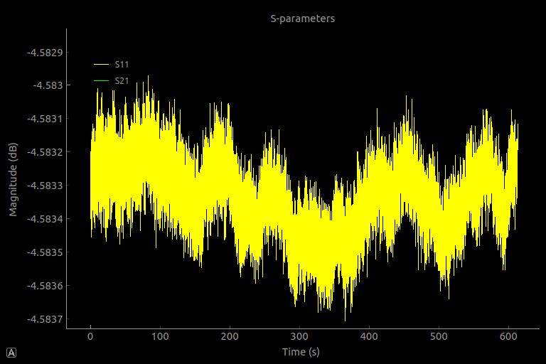
Uncorrected S11 of short at 6 GHz after the VNA temperature has stabilized.
After the temperature has stabilized, the measurements are quite stable. Keeping everything absolutely still, drift in uncorrected short S11 measurements is 0.0001 dB RMS in 10-minute measurement with 100 Hz IF bandwidth. Noise in a single measurement is 0.00006 dB RMS, limited only by the signal-to-noise ratio.
In practice, achieving this accuracy is challenging. Moving the SMA cable changes uncorrected S11 by around 0.03 dB and it doesn't return to the original level when the cable is returned to the original position. Bending the cable can cause even larger changes. Connector repeatability, especially with low-quality SMA connectors, also has an effect on the measurement accuracy. Professional labs use expensive phase-stable cables and precision connectors for this reason.
Measurements
Self-made VNA calibration kit. Thru, short, open, and 50-ohm load.
For calibration kit, I'm using the same self-made short, open, and load that I made for my previous VNA. The calibration standards are measured with a commercial VNA that was calibrated with highly accurate calibration kit, and as a result they should be fairly accurate. Thru is an ordinary SMA through adapter, I don't have any measurement data of it, but that's not an issue since I'm using unknown thru calibration algorithm, which, as the name suggests, does not require a known thru standard.
Bandpass filter
6 GHz bandpass filter.
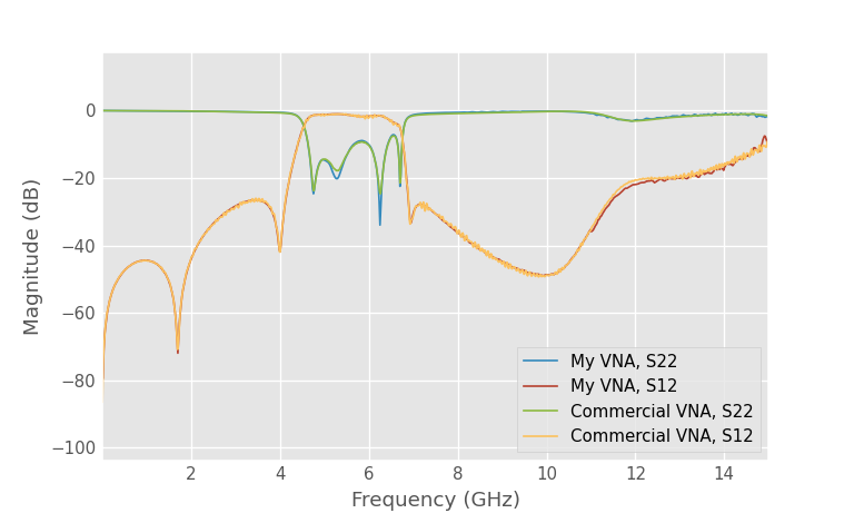
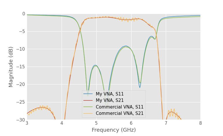
To test the accuracy of the VNA, I measured a 6 GHz bandpass filter with my VNA that was calibrated with the self-made calibration kit. The results were compared to measurements taken with a commercial VNA, calibrated with a proper calibration kit.
The bandpass filter has DEA165550BT-2230C2-H ceramic 6 GHz bandpass filter mounted on an FR4 PCB. Copper sheet was soldered over it to create an enclosure.
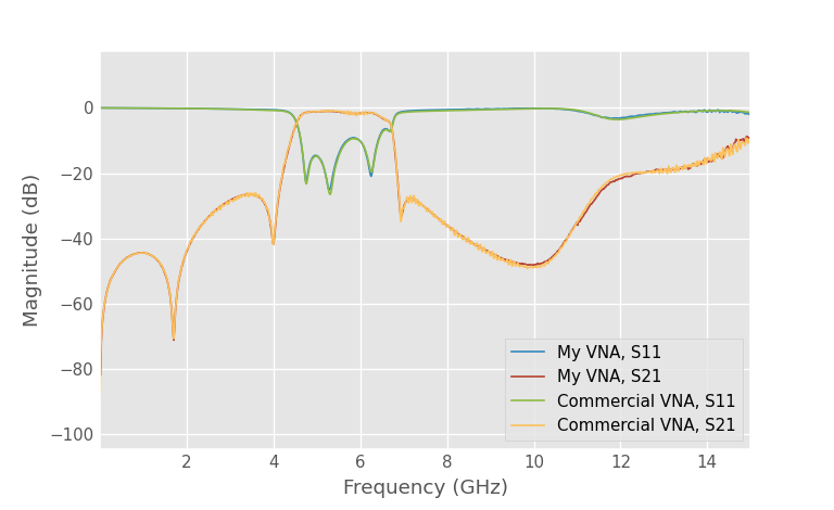
Bandpass filter S-parameters compared.
The S-parameters measured with my VNA closely match with those from the commercial VNA. I only plotted S21 and S11 to make the plot clearer, but S12 and S22 also agree well.
Bandpass filter S-parameters compared, passband detail.
Zooming into the passband, my VNA has less trace noise in the S21 than the commercial VNA. The commercial VNA should be more accurate and I suspect that this is caused by inaccurate thru standard definition in the SOLT calibration. It's old enough that it doesn't have unknown thru algorithm built-in. Ignoring the trace noise measured S-parameters agree with excellent accuracy.
Solved S-parameters of the thru calibration standard.
Unknown thru calibration solves for the thru S-parameters during the calibration. Plotting the solved thru S-parameters, the measurement looks high quality, but the performance of the thru doesn't look very good and it definitely hasn't been designed to be used at these frequencies. Matching is only -8 dB at 15 GHz. S21 trace is also very clean and looks very reasonable indicating that the short, open, and load definitions are correct.
Calibration algorithms
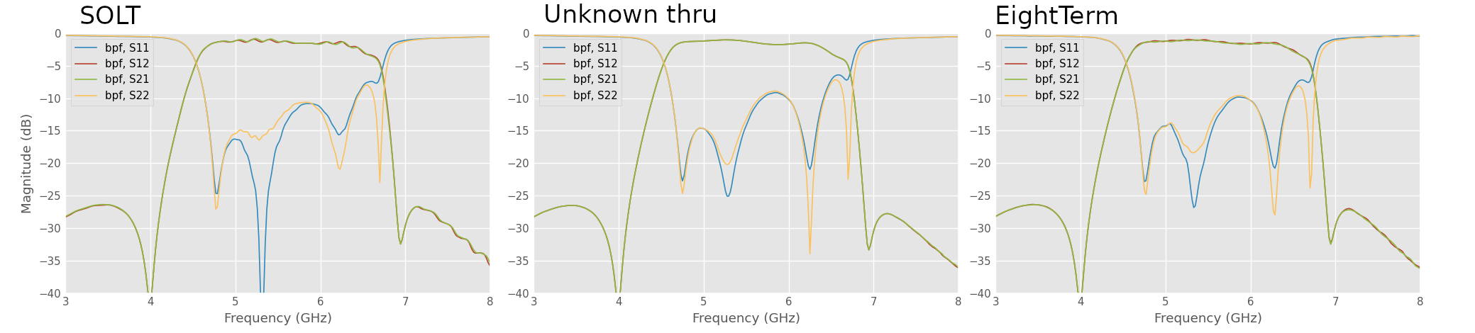
Same measurement calibrated with different calibration algorithms.
Since I saved the raw uncalibrated measurements, I can do the calibration afterwards using different calibration algorithms. I set the ideal thru standard to be a 50-ohm line that is 65 ps long with linear attenuation of 0.1 dB at 4 GHz. This is a simple transmission line model that agrees reasonably well at low frequencies, but the loss and matching differ significantly at higher frequencies. The delay should match well over the whole frequency range.
The SOLT (Short-Open-Load-Thru) calibration algorithm is the default classic VNA calibration algorithm that can also be used with a three-receiver VNA. It requires that all the calibration standards are known accurately. Since the thru standard has errors in this case, the solved S-parameters also have errors. Even though the matching of the thru is -20 dB at 6 GHz, the errors it causes are well above the measurement capability of the VNA.
Unknown thru calibration is likely the best option when calibrating to the end of SMA connectors. It only requires short, open, and load standards to be known, while the thru standard can be completely unknown, as long as it's reciprocal (S12=S21). However, this method requires a four-receiver VNA to measure the switch terms. This measurement is not possible with a three-receiver VNA. When switch terms are known it reduces the number of equations that needs to be solved in calibration by two, allowing some calibration standard definitions to be relaxed.
EightTerm calibration is similar to SOLT, where all the calibration standards are assumed to be known, However, it also includes switch terms, creating an overdetermined system of linear equations. This system is solved least squares, making it a good choice if all calibration standards, including thru, are known to high accuracy.
Both unknown thru and EightTerm calibration are significantly more accurate than SOLT because they have less unknowns to solve for. The thru standard is usually not known with high accuracy in low-cost VNAs, and a four-receiver VNA capable of measuring switch terms is required for these more advanced calibration methods.
TRL calibration
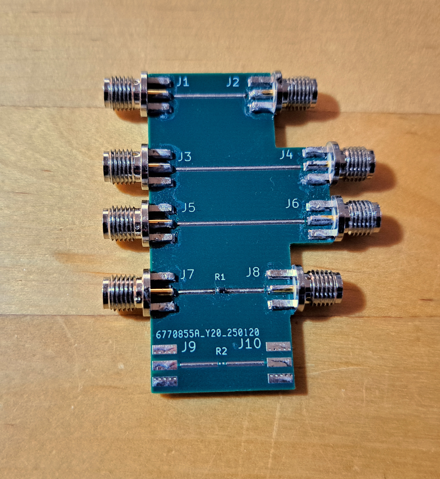
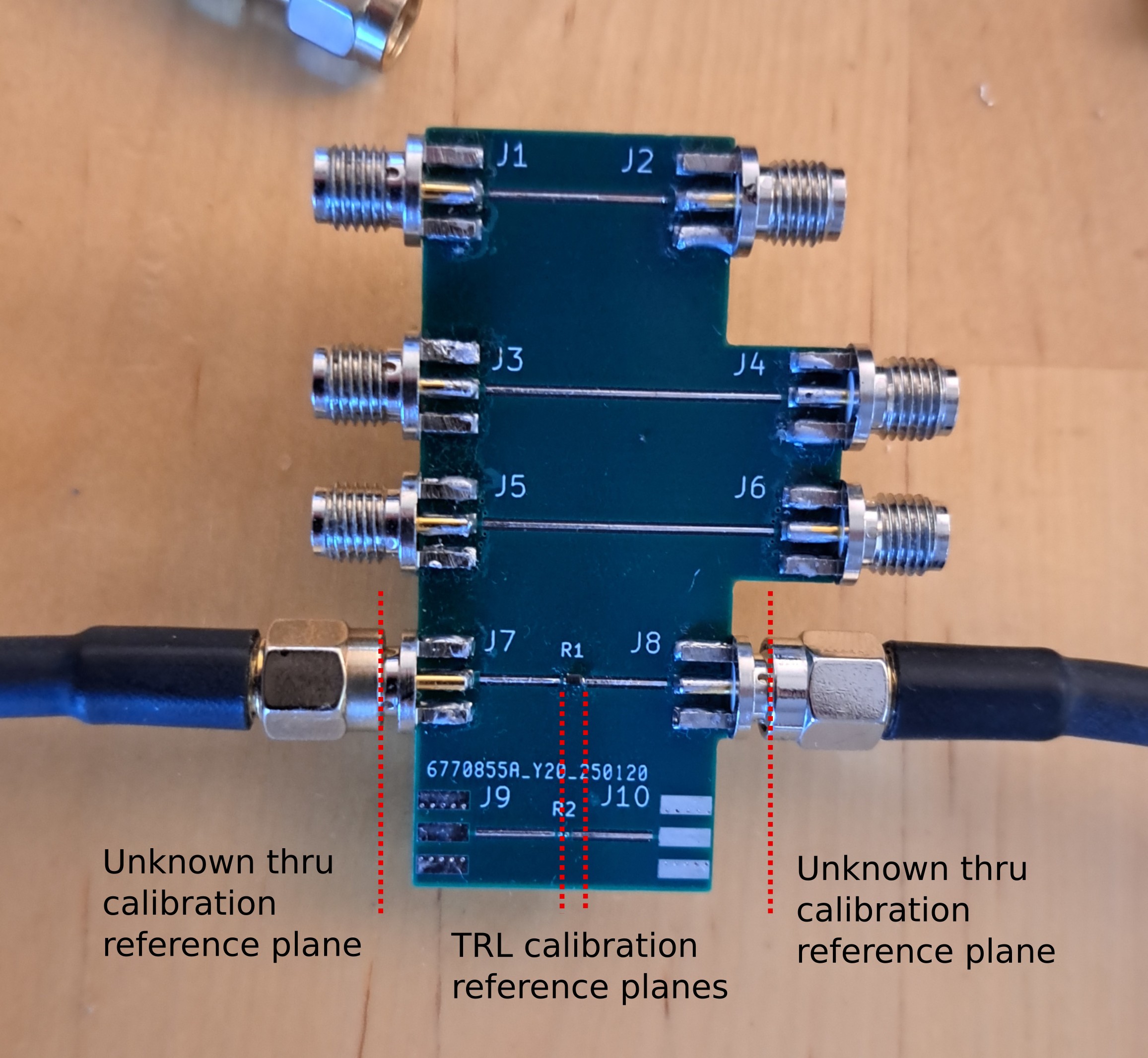
TRL calibration kit and DUT. J1-J2 is thru, J3-J4 is line, J5-J6 is another line with different connector footprint for testing, and J7-J8 is a diode that can be measured with the TRL calibration.
One especially useful calibration algorithm is thru-reflect-line calibration. It requires a four receiver VNA, but it's also possible to use it as a second-stage calibration with three receiver VNA. As the name implies, calibration standard are not the usual short, open, and load. Instead they are two different length transmission lines and reflect. Transmission lines need to have the same propagation constant and optimally the length difference is 90 degrees. Transmission line parameters don't need to be known and reflect can also be unknown but should be identical in both ports.
This is very useful calibration algorithm for measuring devices on PCB, as it allows the VNA reference planes to be calibrated on the PCB right next to the component being measured. It also solves for the transmission line propagation constant and can be useful just for characterizing transmission lines without requiring any calibration standards.
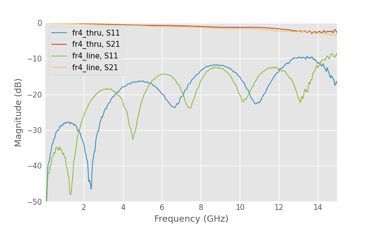
TRL kit thru and line S-parameters calibrated to SMA connectors.
I first measured the lines using unknown thru calibration calibrated to the SMA connectors. This gives some indication on the loss and matching. If the connectors are too reflective it can result in inaccurate calibration as the reflections make it hard to measure the device, but this should be fine.
Some slight ripple is visible in the S11 and S22 measurements, especially above 11 GHz where the 3rd LO harmonic is used. The main reason for the ripple below 11 GHz is due to the measurement cable stability. If I'm not careful with keeping the cables stable the ripple can be even larger.
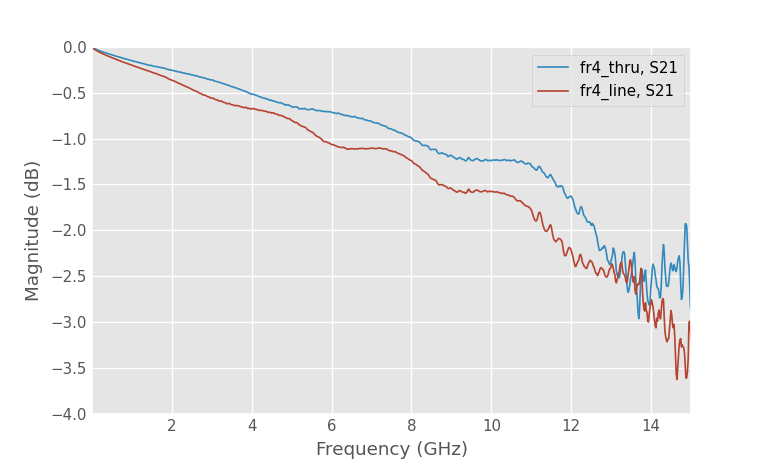
TRL kit thru and line S21 zoom.
Zooming into the S21 trace, it's very clean below 11 GHz. Above this frequency, the 3rd harmonic LO starts to be used resulting in significantly larger trace noise. Some of the trace noise at low frequencies can be caused by the calibration kit definitions that uses measurements instead of models. Any noise in the calibration kit measurement will be transferred to the measurements.
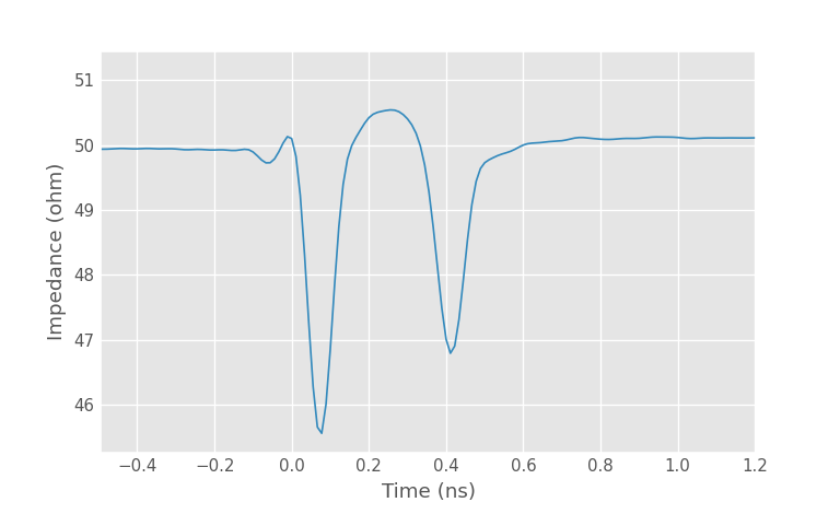
Time-domain impedance step response of the line.
Using Fourier transform, the time-domain impedance step response of the measurement can be obtained. In this case, calculating the time-domain response of the line shows the impedance discontinuities from the SMA connectors and it also gives an estimate for the transmission line impedance, about 50.5 ohms. The mathematical transformation from frequency to time-domain is much easier and accurate than trying to actually sample the reflected waveform at 15 GHz sampling frequency.
The quality of the time-domain transformed data is excellent. With my previous VNA the same measurement would be too inaccurate to be useful.
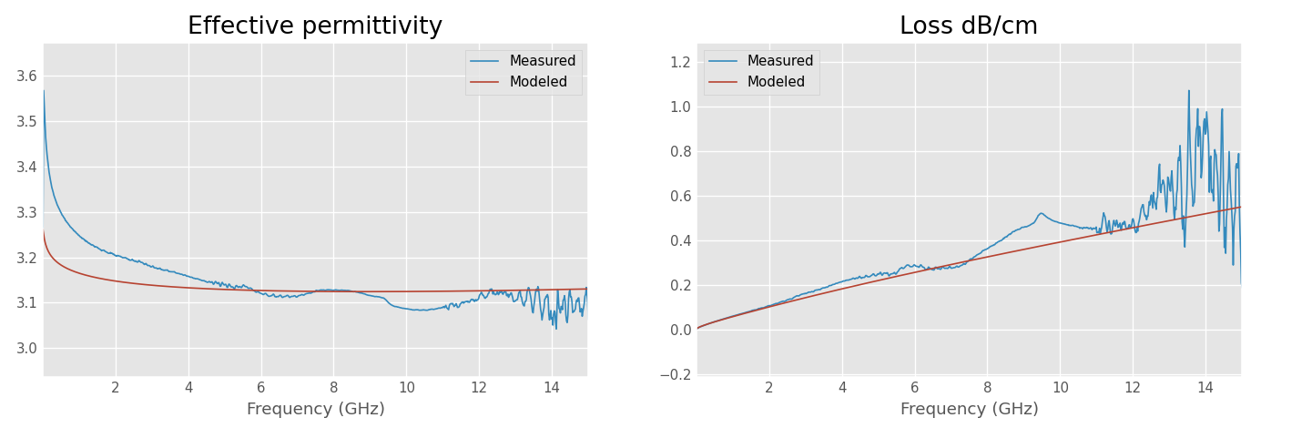
Transmission line parameters solved by the TRL calibration.
TRL calibration solves the transmission line propagation constant during the calibration. It's useful to plot this as effective permittivity and loss per cm. In this case reflect standard can be short calibration standard at the end of the coaxial cable and no separate reflect standard is needed on the PCB.
I also compared these values to microstrip line model using 4.6 substrate dielectric constant and 0.015 loss tangent. These should be about what they are supposed to be and it agrees somewhat okay. FR4 is notoriously frequency dependent material and the model using non-frequency dependent parameters doesn't match over the full frequency range. FR4 dielectric constant decreases and the loss tangent increases as the frequency increases.
This isn't quite ideal test setup for characterizing the transmission lines since the length difference between thru and line is just 9 mm. This small length difference leads to small differences in the S-parameters and makes the measurement sensitive to noise, measurement errors, and differences in the connector S-parameters. Especially with these low-cost SMA connectors I'm using there can be some small difference between thru and line SMA connectors, which cause errors in the solved transmission line parameters. I don't think the peak at 9 GHz for example is caused by VNA measurement accuracy, and it's more likely to be due to differences in the SMA connector S-parameters. FR4 substrate also isn't uniform due to fiberglass wave construction and two identical lines at different places in the weave can have slight differences.
Repeatability also impacts the accuracy of TRL calibration. This TRL kit was designed for frequencies up to 6 GHz, and the solved transmission line parameters remain accurate up to that frequency. The TRL calibration should also maintain its accuracy up to this frequency. Beyond that the calibration is likely not as accurate.
Varactor diode measurement
Varactor diode measurement setup.
With the TRL calibration it's possible to calibrate the VNA right next to the component being measured on the PCB. This allows accurately characterizing SMD components.
The varactor diode on the PCB is SMV2020-079LF. It's a diode whose capacitance changes as the reverse bias voltage across the diode is varied. They are used, for example, in voltage-controlled oscillators.
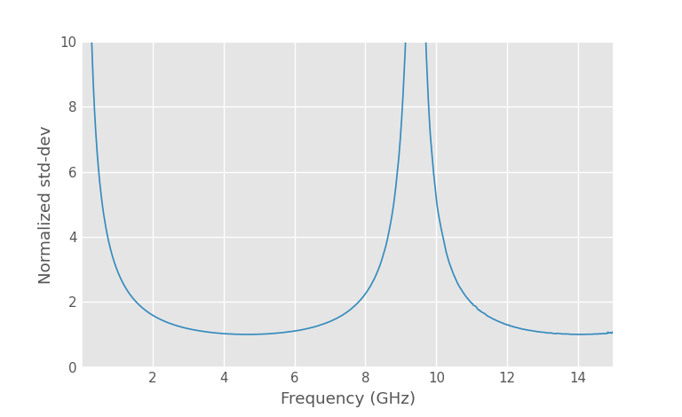
Normalized standard deviation of the TRL calibration.
TRL calibration accuracy depends on the phase shift between thru and line standards. It's best when the phase shift is ±90 degrees and extremely poor when the phase shift is 0 or 180 degrees. The theoretical effect on calibration results can be quantified by calculating the normalized standard deviation of the noise in result, normalized to the best case of 90-degree phase shift. In this case, the best accuracy is around 4.6 GHz, and poorest at 9 GHz due to the line length being 180 degrees at that frequency.
I didn't have this good VNA when I made this PCB, so I didn't think to include a second shorter line to extend the calibration maximum frequency. With this TRL kit, measurement accuracy will be poor around 9 GHz.
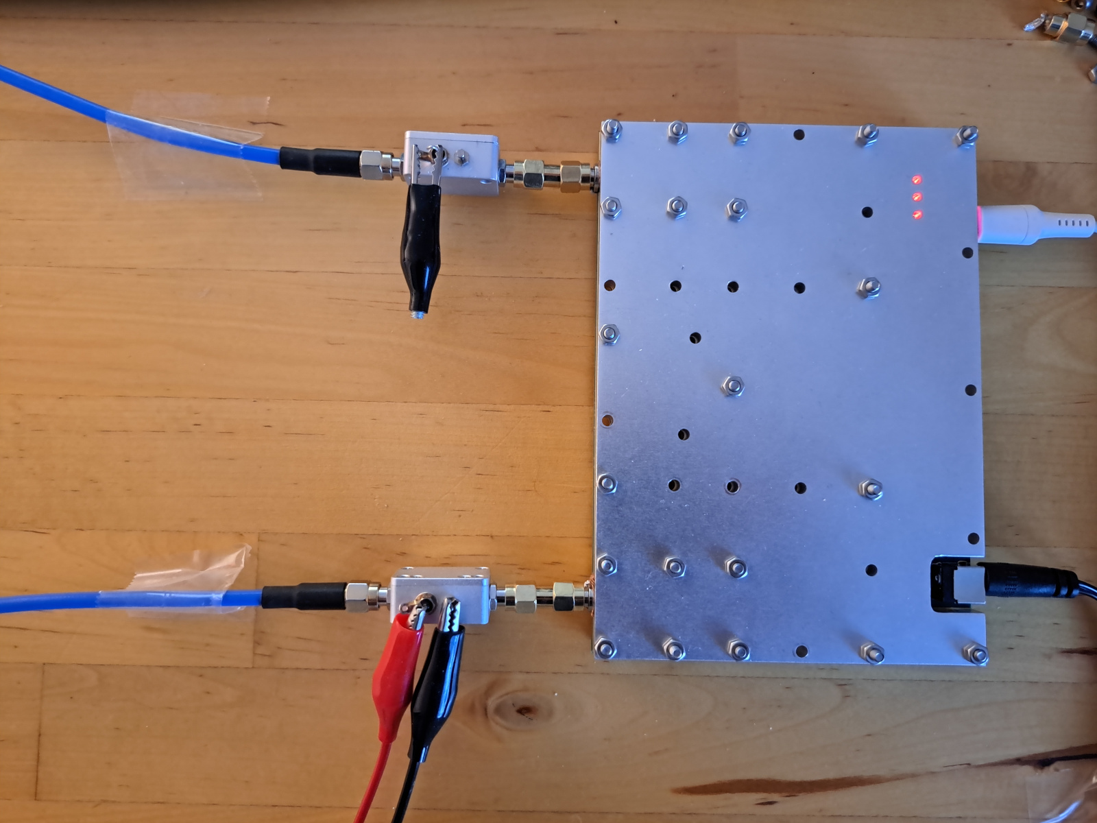
Bias-T's added to VNA ports for biasing the diode.
To measure the diode S-parameters at different bias voltages, I added bias-T's to both VNA ports. Adding them close to VNA is better for stability, and taping down the SMA cables minimizes their movement during measurement, improving stability.
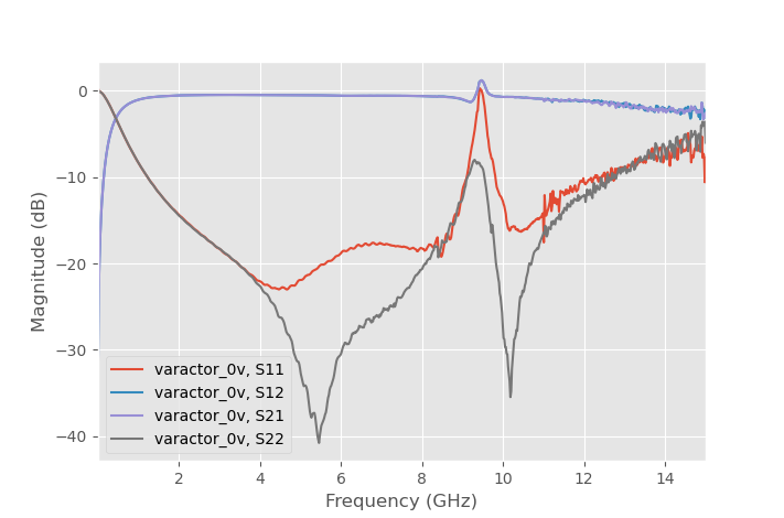
S-parameters of the diode with 0V bias with TRL calibration.
9 GHz calibration singularity severely affects the results, but the S-parameters are clean before and after it. TRL calibration accuracy is also poor at low frequencies, but due to higher SNR, better stability, and better connector repeatability at low frequencies, it doesn't cause similar issues.
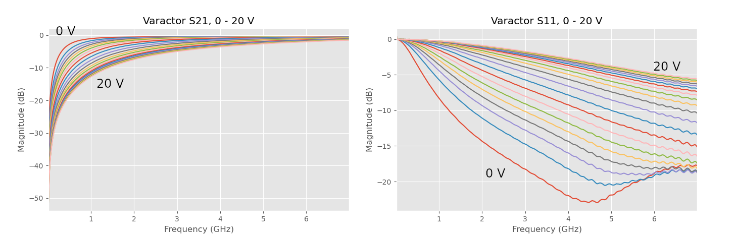
Diode S21 and S11 measurements at 0 - 20 V reverse voltage.
I measured the diode at 0 to 20 V reverse bias voltage in 1 V increments. The frequency range is limited to 7 GHz to avoid the calibration singularity. The diode is expected to behave like a variable capacitor, with capacitance being the largest at zero bias and decreasing as the reverse bias increases.
This measurement would have requires flipping the DUT after every measurement if I was using a 1.5-receiver VNA. It would have not only been very tedious, but also terrible for measurement accuracy. However, with a proper two-port VNA, the measurement setup can remain static and making the measurement is very quick only taking few minutes.
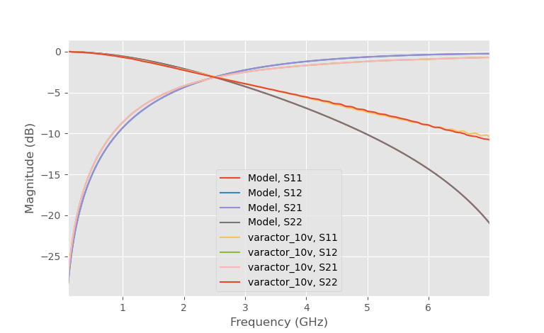
Measurement vs SPICE model at 10 V reverse bias.
The diode has a manufacturer supplied SPICE model. Comparing the measurements to it, the results are quite close at low frequencies but some differences in S11 and S22 can be seen at higher frequencies.
The results can be expected to be at least a little different since my measurement includes PCB pads which are not included in the SPICE model.
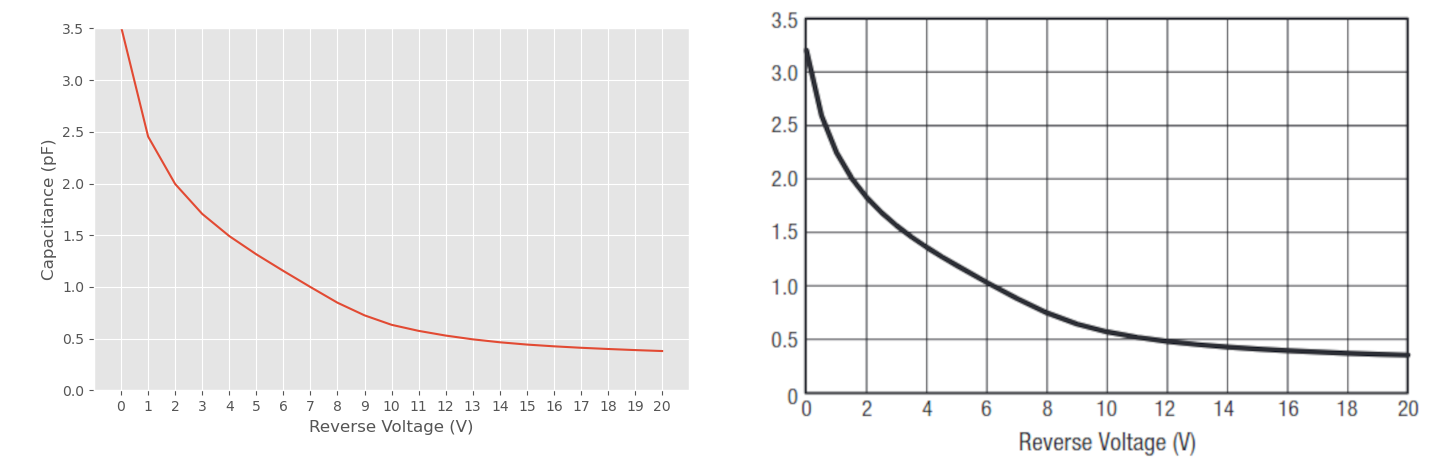
Capacitance vs reverse voltage. My measurement result vs datasheet plot.
When a capacitor is fitted to the measured S-parameters, the capacitance vs reverse voltage graph is very similar to that on the datasheet. However, in my measurement, the diode has few hundred femtofarad higher capacitance at low bias. Some of this discrepancy could be caused by the PCB and it's also possible that there is some manufacturing variation in the diodes.
The diode measurement results have very low noise and the VNA can measure the diodes low capacitance very accurately.
Conclusion
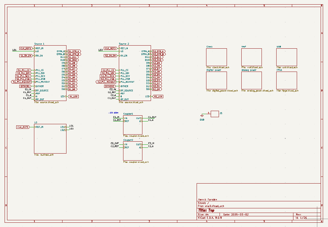
Schematic of the VNA (click to open).
The designed VNA has excellent measurement quality, easily surpassing all of the existing low-cost VNAs. It has four receivers which makes advanced calibration methods, such as unknown thru possible. Isolation is excellent, over 120 dB, and the source frequency range is 10 MHz to 15 GHz.
The total cost of components in prototype quantities was $300, PCBs cost $100 for five pieces, and the CNC machined case was $75 (excluding taxes and shipping). The couplers require some manual assembly, but it should be possible to manufacture this at very low cost. I don't have plans at the moment to manufacture these for sale. The schematic of the VNA is available above for anyone interested in making their own VNA or just curious about the details.