Introduction

FMCW and pulse radar architectures.
I have previously made several FMCW radars that have worked well. FMCW (Frequency Modulated Continuous Wave) radar is quite easy and cheap to make. It uses separate transmit and receive antennas, which avoids the need for switching between receiving and transmitting. It mixes the received signal with the transmitted signal, resulting in a low output frequency, making it possible to use low-speed analog-to-digital converter (ADC). However, big, serious radars typically aren't FMCW radars, instead they are pulse radars. Switching one antenna between transmit and receive modes allows them to use just one antenna. When an antenna diameter is measured in meters it matters a lot how many are needed. Pulse radar can use large transmit power without worrying about saturating the receiver, which is a big issue with FMCW radar. Pulse radar is also better for measuring velocity of fast-moving targets as it can transmit pulses more frequently, resulting in larger maximum unambiguous Doppler shift it can measure.
For these reasons, FMCW radars are usually used in short range applications such as automotive radars and aircraft altimeters, while pulse radars are used mainly for long-range applications such as weather radars, aircraft detection, and synthetic aperture radar imaging from aircraft or satellite.
Pulse radar is much more difficult to design than FMCW radar. To share one antenna, very fast switching between transmit and receive is needed. Radar pulses travel at the speed of light, and for example, if switching from transmit to receive takes 1 microsecond, all the reflections from targets in 150-meter distance would be missed during the switching time. Sharing one antenna causes the radar to have a minimum detection distance, which can be hundreds of meters which makes it unsuitable for short-range operation.
Another difficulty is that pulse radar requires much faster ADC to capture the received pulses. FMCW radar mixes transmitted and received waveforms which results in a low-frequency sine wave for each target at the mixer output, for short-range operation, it's possible to use ADC sampling frequency of 1 MHz or even less while using hundreds of MHz of RF bandwidth. Pulse radar requires much faster ADC, typically fast enough to sample the whole RF bandwidth of the transmitted pulse. The range resolution of the radar is determined by the RF bandwidth, and for useful range resolution ADC sampling rate should be hundreds of MHz or even over 1 GHz. This fast ADCs are very expensive and require expensive digital electronics to handle all the data.
This article is about my experiences building a modern pulse radar utilizing fast digital signal processing cheaply.
Pulse compression radar
There are many kinds of pulse radars, and the one I want to make is a pulse compression radar that supports arbitrary waveforms. Generating only linear frequency sweeps could be simpler and sufficient for many practical applications, but it wouldn't be as interesting.
The requirement for arbitrary waveform means that there needs to be a digital-to-analog converter (DAC) with large enough sampling rate to generate the transmitted waveform. The receiver also needs an ADC with large enough sample rate to sample the whole RF bandwidth.

Radar RF side block diagram.
Above is the block diagram of the radar. The architecture is very similar to software-defined radio (SDR) and it could be used as a radio too. The radar has two time-multiplexed receiver antennas with transmitter being shared with one of them. I added the second receiver channel mainly because it was very cheap, it only requires additional switch, LNA and SMA connector. The second receiver channel makes it possible to use the radar also in FMCW mode.
In a proper radar system some filtering would be useful at both transmitter and receiver, but I left it out here to save money.
Superheterodyne and zero-IF (direct conversion) transmitters. Superheterodyne mixing to IF frequency is done digitally.
TX and RX are zero-IF architecture. This is not ideal from a performance point of view but it's the cheapest option. The output of all mixers contains not only the desired frequency-shifted signal but also local oscillator (LO) leakage and image signals, which is the same signal as the desired one but mixed at the opposite side of the LO frequency. If DAC generated the signal at offset frequency it would be possible to filter out the unwanted frequencies at the mixer output with a bandpass filter, but with zero-IF transmitter these unwanted frequencies overlap the signal, making it impossible to filter them out with a fixed filter.
Similarly, these same nonidealities are also present at the receiver. These nonidealities cause distortion of the received waveform, leading to increased range sidelobes for each target.
While superheterodyne architecture would provide better performance, implementing it would require more hardware and my goal is to make a working system with minimal budget. With zero-IF architecture many of the nonidealities can be compensated sufficiently digitally. Predistorting the DAC output signal can compensate for the mixer nonidealities, resulting in a clean output signal. Receiver output signal can also similarly be modified digitally to remove many of the nonidealities if they can be characterized to sufficient precision.
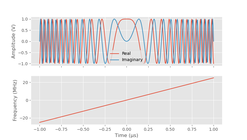
Complex linear frequency sweep signal in time domain and instantenous frequency.
The DAC outputs a complex IQ signal that is modulated by the IQ mixer to the LO frequency and transmitted by the antenna, transmit/receive switch is then switched to receive and reflected signal is sampled by the receiver. Each target reflects some of the transmitted signal and the reflected signal is a sum of the signals from each target.
Complex IQ format allows representing both positive and negative frequencies at the baseband. At the transmitter IQ modulator the I and Q signals are mixed against LO and 90 degree phase shifted LO and summed. The result is that positive baseband frequencies are shifted above the LO frequency and negative frequencies at baseband below the LO frequency.

Pulse compression of the received signal. By correlating with the reference signal the power from pulse is concentrated.
To get the target locations convolution is calculated against the transmitted signal. At the time instance where there was a target the received and transmitted signals correlate and convolution results is large, when there isn't a signal there isn't a correlation and convolution result is small. In practice the convolution is calculated using fast Fourier transform (FFT) as that is faster in practice than calculating the convolution in time domain.
In the above plot sidelobes can be seen around the two targets in the result. These result from the convolution output not being completely zero when the waveform isn't aligned. Multiplying the reference pulse by a windowing function can be used to control the sidelobes of the convolution output. Windowing function can also be applied to the transmitted pulse to further decrease the sidelobes. Drawback of windowing is that it widens the mainlobe and results in slightly worse range resolution. How much sidelobes are traded for resolution can be controlled by the used windowing function.

Range-Doppler processing. Only the amplitude of the pulse is plotted in graph. Phase of the signal is important for Doppler FFT.
Besides the distance to the target, radar can also measure velocity of the target from how phase of the received signal changes during many measurements. By sending a burst of pulses and calculating FFT over the number of pulses dimension, the targets are separated both in velocity and range in the resulting range-Doppler map.
Velocity could be also measured from change of distance, but the beauty of using phase shift of the received signal is that velocity can be obtained from the same measurement as the distance, multiple objects at the same range but with different velocities can be separated, and the measurement accuracy is much better. Detecting multiple objects at the same range with different velocity is important for separating moving objects from stationary objects such as ground, trees, and buildings that can have a large reflected signal that would otherwise mask a small moving object.
Measuring angle of the target would also be possible with multiple antennas, but in this case with one antenna there isn't angle information.
ADC and DAC
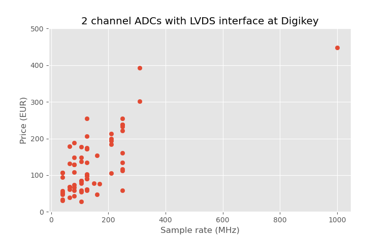
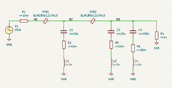
2 channel LVDS interface ADCs with >10 bits, sample rate vs price from Digikey.
ADC sample rate is one of the most important parameters for the system as it determines the maximum RF bandwidth that the system can receive. ADC sample rate should be as fast as is affordable. In general, it's much easier to make the RF side and DAC to have greater bandwidth than ADC, and it's ADC bandwidth that limits the system.
The requirement for ADC is having at least two channels, this is required for IQ sampling, and LVDS output interface. Two one-channel ADCs could also be used but it's disadvantageous from PCB area and routing perspective. The fastest ADCs usually have JESD204B digital interface, the problem with it that it requires high-end FPGA with high-speed serial transceivers and those are in general too expensive for my budget. LVDS is the highest speed interface that can be connected to regular FPGA I/O pins.
In the above plot are all 2 channel ADC with LVDS interface and at least 10 bits. The best sample rate for price is ADS4229 with 250 MHz sample rate for 58 EUR / piece in single quantity. Even higher ADC sample rate would be very desirable, but any higher sample rate than this would get much more expensive. There is one two channel 8-bit ADC with 500 MHz sample rate for 73 EUR / piece, but it has 20 dB lower SNR than the 12-bit ADC and doubling the sample rate would only give back 3 dB SNR. Low bit ADC would decrease the dynamic range of the receiver making it more prone to saturation, and it would require more gain before the ADC, so I decided against using it despite the higher sample rate.
Suitable DACs are easier to find, and I chose to use DAC3174 two-channel 14-bit 500 MHz DAC costing 33 EUR / piece. While the system bandwidth is limited by the ADC, it's useful to have more than enough bandwidth on the DAC to make filtering easier.
ADC filter
ADC requires anti-aliasing filter before it to limit the signal frequency to below half of sample rate (Nyquist rate) to avoid aliasing. To get the largest usable bandwidth the cutoff frequency of the anti-aliasing low-pass filters should be as close as possible to the Nyquist rate, but this makes implementation of the filter difficult as it needs to have very sharp cutoff.
Filter should also have equal amplitude and group delay on the passband. Amplitude requirement is easy to understand, we don't want to have different frequencies attenuated different amounts. Group delay measures how much different frequencies are delayed by the filter. If the group delay difference is too large for different frequencies, the received pulse is distorted by the filter decreasing its correlation to the reference pulse. In practice, this shows up as higher sidelobes.
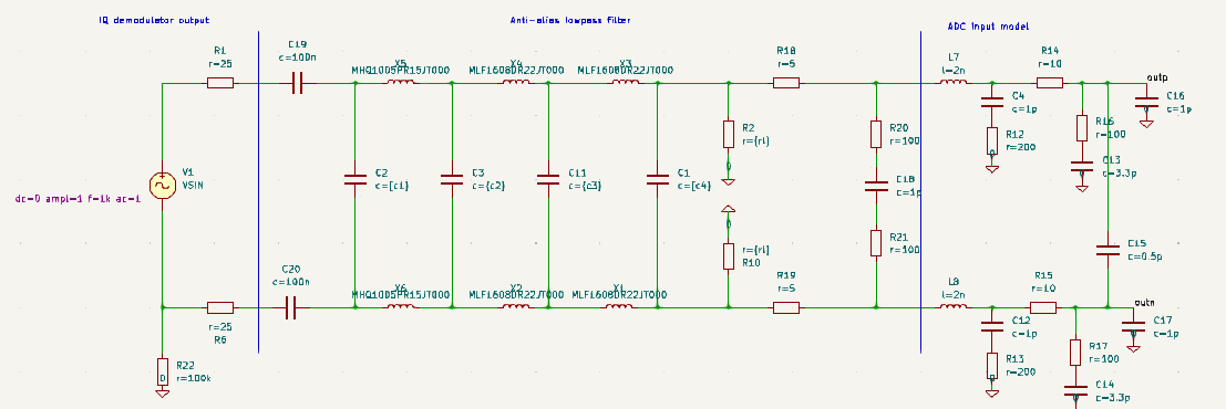
ADC lowpass simulation setup.
Source impedance of the IQ demodulator is 50 ohms differential. ADC input is also differential, and its impedance varies with frequency having high impedance at lower frequencies, but at higher frequencies the input capacitance is significant. ADC datasheet provides a model for the ADC input which I added to the simulation setup. It suggests adding a resistor at the input that sets the input impedance, series resistors to limit ringing due to bond wires and additional resistor and capacitor across inputs to filter sampling glitches. While adding a 50 ohm resistor across the ADC input would be good for filter design perspective it attenuates the signal too much as there already isn't enough gain in the receiver and the IQ demodulator linearity decreases with low output impedance. I added instead 200 ohm resistor to minimize the signal attenuation. This makes the filter design challenging, as the high load impedance requires using small capacitors and large inductors. Higher impedance also increases the effect of sampling glitches, which are caused by ADC input sampling capacitors rapidly sampling the input signal. Adding IF amplifier would have made the filter design easier.
100 nF series capacitors decouple the DC levels of IQ demodulator and ADC. While it would be good to have DC coupled signals, the DC levels of IQ demodulator and ADC are different and any significantly different DC levels would limit the maximum AC signal range.

Simulated frequency response of the ADC lowpass filter. Nyquist frequency marked with vertical line.
The cutoff frequency of the filter is set at 100 MHz and there should be -20 dB attenuation at the Nyquist frequency of 125 MHz. Up to about 60 MHz both magnitude and group delay are very good, above that it could be better but its hard to improve with these constraints. There is some variation in the passband magnitude that would have been smaller with 50 ohm impedance. Group delay is relatively good at medium frequencies, at very low frequencies AC coupling capacitor causes the delay to shoot up and near the cutoff frequency there is a peak in the delay. The filter response can be compensated digitally if its a problem.
DAC anti-alias filter

Simulated frequency response of the DAC lowpass filter. Nyquist frequency marked with vertical line.
Digital-to-analog converter is also a sampled system, and it has unwanted aliases at the output that need to be filtered out. The sample rate of DAC is 500 MHz which compared to required signal bandwidth of 100 MHz makes the filter design much easier. The alias frequencies are in the range 400 to 500 MHz for 0 to 100 MHz signal.
The filter is designed to have flat magnitude and group delay below 100 MHz and in the simulator both look very good. Cutoff frequency is just above 100 MHz so that the peak in group delay is above 100 MHz. The aliases are much further away in frequency than with the ADC, and they are attenuated at least 65 dB more than the signal. This amount of attenuation is more than enough for the DAC aliases to not cause any issues, but it does mean that they are visible at the RF output. If the signal power is 30 dBm, then the image signal is about -35 dBm. For proper radar the attenuation likely should be higher to avoid radiating power at other than the allocated frequency band.
FPGA
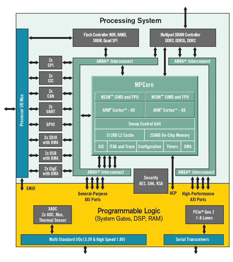
Xilinx Zynq FPGA block diagram. The chip has two-core ARM CPU and programmable logic with fast interconnect between them.
Using just a microcontroller isn't possible for this application. FPGA is required for accurate timing of pulse generation and for managing the ADC and DAC data. Accurate timing of pulse generation is critical for proper operation. Switching between transmit and receive needs to be done quickly and accurately, any timing error in pulse triggering or in the receiver will be visible as large distance error.
Pricing of the FPGAs is very bizarre. Looking at Digikey or other resellers many of the suitable parts have prices starting in hundreds of dollars and better ones can cost several thousand. However, the exact same parts can be found for fraction of price from China. For some reason, Zynq 7020 is one of the cheapest Zynq FPGAs in China available at $17, while the exact same part from Digikey costs $173.
Zynq 7020 has dual-core ARM-A9 CPU and typical FPGA programmable logic in the same package. Having also a CPU core is useful as it can handle communication to PC. It can also run Linux and I added SD-card for Linux file system if I want to use it, but initially software is running without any operating system.
Digital design

Block diagram of digital interfaces.
With fast ADC and DAC moving a lot of data, it's important to consider whether the system can keep up. In the above block diagram, digital interfaces between important blocks have been drawn. The FPGA SoC consists of two parts: processing system (PS), which is dual-core ARM A9 CPU, and programmable logic (PL), which is programmable FPGA fabric. They are connected to each other through with four 64-bit AXI buses. Their clock frequency is configurable and, in this case, it's set to 130 MHz which is near the upper limit that it can work. One AXI bus is reserved for ADC Direct Memory Access (DMA) and other for DAC DMA, there's also a third, lower speed AXI bus (not drawn in the diagram) for configuring the registers in the programmable logic.
A fast connection to the PC is needed to quickly transfer captured ADC samples. Initially, the digital processing will be done on PC, but it should be possible to do it on FPGA too for some applications. If the interface to PC is much slower than the ADC data generation rate, it limits how often the radar can be triggered. For target tracking, this means slower update rate of target positions.
1 Gbps Ethernet is the fastest interface to PC that can be easily connected to this FPGA chip. USB 3 is another possible choice, offering 5 Gbps speed with easy connection to PC, but it would require an external USB 3 transceiver chip and more effort to make it work.
The system has a single DDR3 DRAM chip that is connected to the PS side of the FPGA. While the memory chip could be clocked faster, the memory interface speed is limited by the FPGA memory controller to 1066 MHz. Memory bus width is 16-bits. The memory controller supports up to 32-bits, but it would require adding a second DDR3 chip and the higher bandwidth is not necessary in this system.
ADC samples are received by the PL side, which has a small FIFO buffer and DMA controller transfer them to DRAM through the PL side. DAC also has its own DMA channel, but DMA uses only one AXI bus limiting it to 8.3 Gbps, which is less than what the DAC needs. It's also important to note that DDR3 bandwidth is less than the sum of the DAC and ADC bandwidths, making streaming DAC samples from DRAM while storing ADC samples at the same time impossible. For this reason, there is a small 1 MB memory on the PL side that stores DAC samples. Pulse samples are transferred from PC to DRAM through Ethernet, then DMA transfers them to the small memory on the PL where they are transferred to the DAC every pulse.
A small DAC memory limits the pulse length to 130 µs, but it's plenty for pulse radar. A 130 µs pulse corresponds to 20 km minimum detection distance, and typical pulse length is about 1 µs. The pulse could also be generated on PL, eliminating the need for memory, but lookup table implementation makes it easier to change pulse parameters such as windowing function, pre-distortion, and test different types of pulse waveforms.
RF design
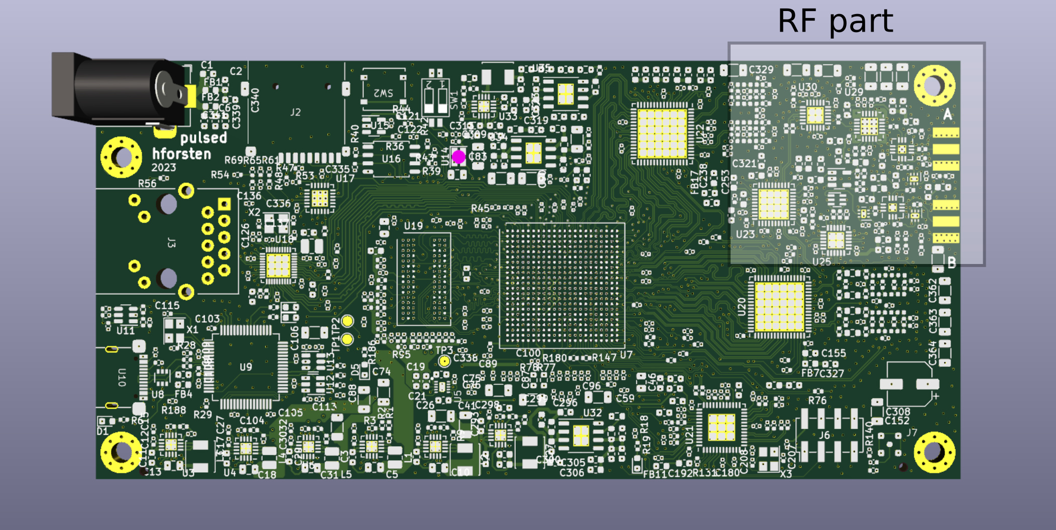
RF parts take only a small portion of the PCB area. It's also a small amount of required work on the project although it seems like it should be the important part.
With the digital parts out of the way it's time to look at the RF side. Designing the RF parts is relatively straight forward. Similar to my previous radars, the operating frequency will be around 6 GHz. This is the highest frequency with many off-the-shelf cheap components due to many consumer applications.
RF part consists of: IQ modulator, IQ demodulator, PLL for generating the LO frequency, power amplifier, low noise amplifiers and switches.
IQ modulator should have low LO leakage, high image rejection, enough output power to drive PA without needing another amplifier, and baseband voltage level compatible with the DAC output voltage range. There aren't that many possible commercial chip alternatives and most of them are very similar in performance. Same applies also to the IQ demodulator.
Choosing a power amplifier was more difficult. While big, expensive radars often have transmit power measured in kW or even MW, but that's unrealistic in this case. I would like to have at least 1 W peak RF power but there are surprisingly few choices at 6 GHz band despite WLAN applications that require power amplifiers. The best suitable amplifier I found was Skyworks SE5004L, which has 2 W typical output 1 dB compression point and high gain of 32 dB, but its documentation is severely lacking. There isn't any graph of gain vs frequency and it requires some external components, but there aren't any values for them in the datasheet. The solution for external components is found in the SE5004L-EK1 evaluation kit documentation, which has the schematic of the evaluation board of this chip. It's also out of stock at the moment at common resellers although it's available at some Chinese resellers. In the end I did decide to go with it because there aren't many other cheap alternatives with enough output power.
Switching speed of the T/R switch is very important, and it should have high enough power handling capability to handle the 1 W power amplifier output without blowing up or distorting the signal. Especially the fast switching speed is a though requirement that rules out many options. I ended up choosing MASW-007588 switch that has 55 ns switching speed and 37 dBm 1 dB compression point. While 55 nanoseconds is fast, in that time light travels 16.5 meters. There are better switches specifically made for this kind of applications, but they are too expensive for my budget.
Another option would be to use circulator instead of switch. This is common for higher power radars as circulators can handle hundreds of Watts of power, and there is no switching speed. There are some circulators for this frequency, but big issue with them is that they are very large and much more expensive than simple switch.
The receiver should have enough amplification that the RF noise floor is above the ADC quantization noise floor. The RF noise floor spectrum at the ADC input can be calculated as \(kT\), where \(k\) is the Boltzmann constant and \(T\) is temperature in Kelvin. This results in power density of about -174 dBm/Hz at room temperature.
LNA amplifies the thermal noise and adds some noise to it which is determined by LNA's noise figure. Switches and PCB lines have some losses. IQ demodulator's voltage conversion gain can be used to calculate the output voltage density at the ADC input.
ADC noise floor can be calculated from SNR specification, 69.4 dBFs (decibels relative to full scale) in this case, sample rate 250 MHz, and maximum input voltage 2 V peak-to-peak (0.707 Vrms). Noise is then 69.4 dB below 0.707 Vrms maximum input voltage for each sample, and there are 250 million samples in one second which equals bandwidth of one Hertz. This gives the ADC noise floor density of -156 dBV/Hz.
Calculating the RF noise floor at the ADC input after considering the whole signal chain from starting from LNA gives noise floor of about -155 dBV/Hz. This is barely not enough gain. RF noise floor should be much higher than the ADC noise floor, typically about 10 dB, so that the ADC quantization noise doesn't increase the noise of the whole receiver. An ADC driver amplifier could easily have enough gain, but low-frequency amplifiers with high enough bandwidth are surprisingly expensive. In the end, I just decided to have few dB higher noise floor.
Maximum detection range
The maximum detection range of the radar can be calculated as following:
The transmitter transmits a pulse of length \(t_s\) with average power of \(P_t\), which is radiated by the transmitter antenna with gain \(G\). The power density (\(W/m^2\)) at distance \(r\) can be written using Friis' equation as \(P_t G / (4 \pi r^2)\). This power is reflected by a target with a radar cross-section of \(\sigma\) and some of it is reflected back to the radar. The received power depends on the effective area of the receiving antenna: \(P_r = P_t G A_e / ((4\pi r^2)^2)\). \(A_e\) can be written in terms of the antenna gain as \(A_e = \lambda^2 G / 4 \pi\), where \(\lambda\) is the wavelength of the RF signal. The equation for the received power at the receiver input can be written as:
This is the received power from one pulse. To increase the received power, multiple received pulses can be coherently summed. It's important that the summation is coherent so that the phases of the received pulses are aligned. In practice, instead of summing, an FFT is used so that power from moving targets can be coherently summed and separated from each other.
To get the maximum detection range, we need to find the minimum detectable received power. The detection performance is limited by the noise of the receiver. Thermal noise density (W/Hz) of the receiver is \(kT\), where \(k\) is the Boltzmann constant and \(T\) is the receiver temperature in Kelvin. The receiver amplifies this thermal noise and adds its own noise to it. The noise factor, \(F\), of the receiver is how much higher the noise floor of the output is compared to theoretical thermal noise floor if there wouldn't be any added noise. This can be calculated from the receiver gain, RF amplifier's noise figure and ADC's noise floor.
To get the noise floor, we need to multiply the thermal noise density \(kT\) by the receiver noise factor \(F\) and the receiver's noise bandwidth \(B\). The correct noise bandwidth to use is the minimum bandwidth after all the signal processing which noise can't be separated from the signal. For example, by taking the Fourier transform of the input signal, we can discard all the frequency bins that are beyond where our signal is, and noise at those discarded frequencies won't affect the detection capabilities of the receiver. Pulse compression ideally collects all of the power of a pulse within a bandwidth of \(1/t_s\) for a linear frequency sweep. However, in practice, FFT windowing functions and any mismatch between reference and received pulses will decrease this slightly.
The minimum detectable signal should be higher than the noise floor by some margin. The threshold value for detections can be chosen freely, but there is a trade-off: if we accept detections that are only just above the noise floor, occasionally some of them may be false detections resulting from noise just happening to be above the detection threshold. The probability of false alarm depends on the method used to estimate the signal-to-noise ratio of the detection. For an ideal detector, the false alarm probability can be calculated based on the probability that normally distributed noise is above the detection threshold. Common threshold value is usually around 13 to 15 dB.
At the maximum detection distance the received power is equal to minimum detectable signal:
,where \(n\) is the number of pulses, and \(S\) is the detection threshold compared to the noise floor. Solving for \(r\) gives the maximum detection range:
| Variable | Explanation | Value |
|---|---|---|
| \(P_t\) | Transmitted power | 30 dBm |
| \(G\) | Gain of antennas | 14 dBi |
| \(\lambda\) | Wavelength | 5.2 cm |
| \(\sigma\) | Target radar cross-section | 1 m² |
| \(T\) | Receiver temperature | 290 K |
| \(t_s\) | Pulse length | 1 µs |
| \(n\) | Number of pulses in burst | 1024 |
| \(F\) | Receiver noise figure | 5 dB |
| \(S\) | Detection threshold | 15 dB |
In the above table are estimations of the radar system parameters. Plugging these values in the equation gives a maximum detection distance for target with 1 \(m^2\) radar cross-section of 1200 meters. This might be slightly optimistic, as there are losses in the cables to antennas, loss from antenna efficiency, losses from mismatch, and atmosphere attenuation. However, the maximum detection distance should still be about 1 km. At this maximum distance the average received power from a target is equal to the minimum detection threshold. Therefore, on average, a target at this distance is detected 50% of the time. Due to normally distributed noise, there is a chance that a target at shorter distance is not detected, and a target at longer distance could be detected. However, because of the fourth power dependence of the received power, the probability of detection drops quickly at larger distances.
PCB design

Simplified PCB block diagram. PLL generates 6 GHz RF local oscillator and clock generator generates clocks for ADC, DAC and FPGA.
Practical implementation of the system requires designing a printed circuit board (PCB) that integrates all the components. The system has both RF and high-speed digital circuits that require careful PCB routing to make sure that they function correctly.
The PCB has six layers, and I don't think the FPGA can be routed with any less layers. The material is standard FR-4, which isn't ideal for RF routing since it's quite lossy, but it isn't a big issue in this case since the RF trace length is kept very short.
DDR3 routing
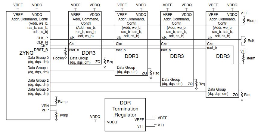
DDR3 routing implementation. Source: UG933
DDR3 DRAM memory connected to the PS side of the FPGA runs at 533 MHz clock frequency with two transfer per clock cycle. The memory uses the DDR3L standard, which is a low-voltage version of the DDR3 standard with a 1.35 V operating voltage instead of the normal DDR3 1.5 V supply voltage. While this isn't very fast by the modern standards, it still requires some care with the routing. Memory traces should be length matched, have correct characteristic impedance, and be terminated properly to minimize reflections.
The nominal characteristic impedance of DDR3 traces is 40 ohms. A shared address bus is fly-by routed to all memory chips and terminated with a 40 ohm resistor to VTT supply, which is at half of the memory supply voltage. Each memory chip has its own data traces with on-chip termination. There are also few control lines that are routed to all memory chips. With only one memory chip on the PCB, the routing is much simpler.
The memory bus can be simulated with circuit simulators before being manufactured. Professional programs have ways to do finite element simulation of the PCB, but this is quite difficult with open source software. FPGA and memory chip driver and receiver electrical models are provided as IBIS files. I used KiCad to design the PCB and it's supposed to include IBIS support but it was unclear how to use it. I ended up using SPISim_IBIS web app to convert the IBIS models to SPICE netlists and simulate them with ngspice.

DDR3 memory routing simulation of a single trace.
I was interested in simulating if address bus termination resistors can be left out in this case where there is only one memory chip, and it's mounted close to the FPGA. I have seen this done on at least one FPGA development board, and it would save some PCB space if termination resistors could be left out.

DDR3 databus with 40 ohm line and termination.
Normally, an eye diagram is used to analyze the timing margin of the memory bus. However, it's not easy to simulate it with ngspice, so I just added a pulse source and did a transient simulation plotting the voltage at the memory chip input. With 120 ps line delay, 40 ohm line impedance, and termination resistance the memory chip input voltage looks fine. High and low thresholds are 0.81 and 0.54 V according to the memory chip datasheet, and the signal looks very good in the simulator.

DDR3 databus without termination resistors.
Without termination resistors, the voltage looks fine from the threshold level point of view. However, there is significant under and overshoot. Supply voltages are 0 V and 1.35 V, and the memory chip input voltage overshoots by about 0.7 V, which is enough to forward bias the ESD (Electrostatic discharge) protection diodes of the memory chip. This might be fine in practice, but memory chip datasheet says that the overshoot should be limited to maximum of 0.4 V. For this reason, I added the address line termination resistors.

DDR3 databus with 60 ohm line and 50 ohm termination resistors.
While removing the termination resistors violates the datasheet guarantees, it's possible in this case to use 60 ohm line impedance and 50 ohm termination resistors with minimal difference in the signal integrity. The benefit of using higher line impedance is that it results in narrower line on PCB allowing for denser layout. A 40 ohm trace is 0.24 mm wide, while 60 ohm trace is 0.10 mm wide. Using narrower trace also allows having more distance between different traces, which decreases cross-talk between traces. 50 ohm termination resistor is close enough to the trace impedance, and since 50 ohms resistors are needed on other places on the PCB, using 50 ohm resistor allows removing one resistor value from the bill of materials, making the assembly slightly cheaper.
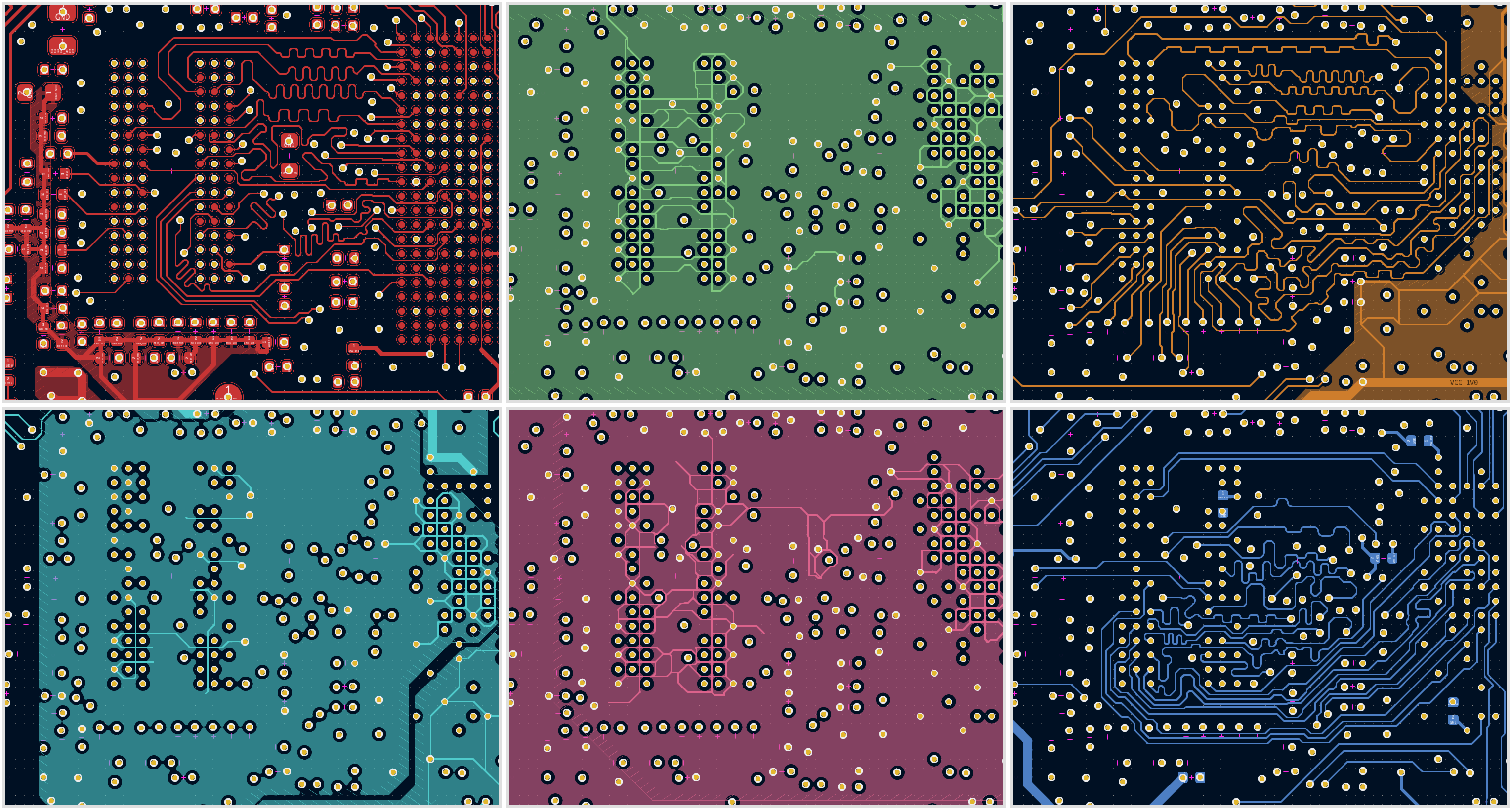
DDR3 routing. FPGA on the right and DDR3 chip and the termination resistors on the left. Top left is the top layer and bottom right is the bottom one advancing horizontally.
Above is the final DDR3 routing on all the PCB layers. Layers 2 and 5 are ground, 4 is supply voltage, and others are reserved for signals. Two grounds are needed for correct impedances on the top, middle, and bottom traces of the PCB. With only one ground plane, the distance from the signal to ground would be too large on either the top or bottom layer. Data bus traces are swapped within the byte boundary to make the routing easier. The traces are length-matched with squiggly lines, and some traces are manually drawn on the ground and supply layers to decrease the size of slots in the planes due to vias. The trace matching requirement is ±10 ps according to the Zynq PCB design guide, which is approximately ±2mm in trace length. However, considering the faster memory chip and having only one memory chip, the actual margin should be much greater. There is also some delay difference inside the FPGA package which should be considered in the length matching.
Transmission line termination
The T/R switch needs to be switched as fast as possible to minimize dead time between transmit and receive, and the same applies for the IQ modulator enable pin. The FPGA I/O pin driver strength can be controlled, and with the highest drive strength it has a rise time of about 400 ps at the switch input in simulator. However, few centimeters of PCB trace between the FPGA and switch input functions as a transmission line, which has significant effect at these frequencies.
The switch input pin is not matched to 50 ohms, and a typical CMOS input has high input impedance. This causes reflections, which severely distorts the switching waveform.

Termination of switch input with capacitor and resistor.
To minimize reflections, the transmission line should be terminated to the characteristic impedance of the transmission line, which is 50 ohms in this case. Placing a 50 ohm resistor to ground near the switch input pin would work, but it would sink DC current and cause the DC voltage to drop. Termination to supply voltage has a similar issue except that now voltage can't reach 0 V.
Termination with a 50 ohm resistor in series with a small capacitor solves the DC level issue. Capacitor value should be tuned so that high-frequency reflections are absorbed without affecting the low frequencies too much.

Simulation of switch voltage with and without termination.
Above is the simulated voltage at the switch input. Transmission line length was 300 ps, and termination capacitor was set to 12 pF. Without termination there is significant over and undershoot, and a risk that the voltage drops below the threshold voltage slowing the switching. With the termination, the waveform is much cleaner.
Power supply
Analog electronic components are sensitive to supply voltage noise. This is especially important for RF receiver with input signal at the level of the thermal noise floor.
Switching regulators have good efficiency, often around 90%, but their output has switching noise that is significantly higher than the thermal noise floor. If this noise isn't filtered properly, it will couple into the received and transmitted waveforms and cause interference at the receiver. A linear regulator, often called low-dropout regulator (LDO) for historical reasons, functions as a variable resistor, dissipating enough power to ensure that the output voltage is at the correct level. The output noise is much lower, but if the voltage drop is too large the efficiency is terrible.
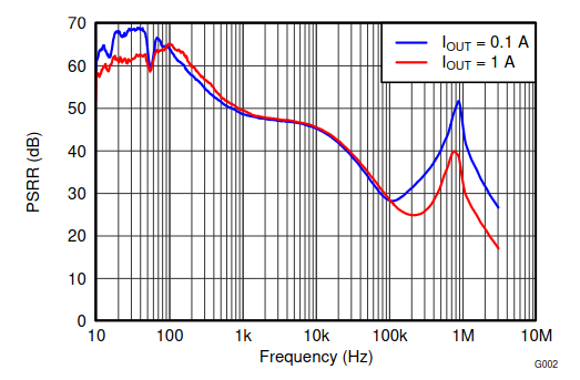
Power supply rejection rate (PSRR) of TPS7A7001 LDO.
To have both good efficiency and low noise, it's common to have a switching regulator followed by an LDO to filter the switching noise. However, this isn't enough filtering in this case. LDO filters well very low frequencies, but it's filtering capability drops at the higher frequencies. Above is the power supply rejection ratio (PSRR) of the LDO I'm using. For example, with a 1 mV amplitude, 2.5 MHz signal at the LDO input is attenuated by about 15 dB, resulting in about 200 µV amplitude signal at the output.
The requirement for minimum power supply filtering can be obtained with few assumptions about the coupling of the noise. The smallest signal level is at the input of the receiver LNA. The thermal noise floor is -174 dBm/Hz at room temperature. With a 10 ms measurement time, the bandwidth is 100 Hz. This results in a maximum of -154 dBm power at the LNA input. At 50 ohm impedance, this corresponds to 5 nV RMS voltage. If the LNA supply voltage is modulated by noise, it affects the gain of the amplifier, and the supply voltage noise is mixed to the RF signal. In practice, the allowed noise amplitude can be larger since there is usually some power supply rejection at the LNA for low-frequency supply voltage noise to the output RF frequency, but it's usually not specified in the datasheet. With a 10 mV worst-case switching noise amplitude, the required attenuation is 120 dB to reach the noise floor. LDO can be assumed to filter about 10 dB, and we can assume another 10 dB power supply rejection from the RF components, which sets the power supply filtering requirement to 100 dB.
Two-stage ferrite bead filter schematic. Capacitor parasitics drawn individually.
The required power supply filter can be designed with ferrite beads. They are inductors that are lossy at high frequencies. A capacitor is needed after the ferrite bead to complete the low-pass filter. The series resistance and inductance of the capacitor are crucial at these frequencies, and they are included in the schematic, assuming an SMD ceramic capacitor.

Ferrite bead filter frequency response.
The above filter achieves 100 dB attenuation at 1 MHz. The switching frequency is 2.5 MHz, and this filter works well at that frequency. However, it has a resonance at 30 kHz, which increases the noise at the output at that frequency. This is caused by the ferrite bead behaving like an low-loss inductor at low frequencies which resonates with the capacitor due to a lack of resistance that would dampen the resonance. It can be fixed in two ways: adding resistance in series with the capacitor or increasing the capacitance. Resistance could be also added in series with the ferrite bead, but this is possible only if the DC current is small.

Ferrite bead filter frequency response with 20 µF first capacitor and 200 µF second capacitor.
With larger capacitors, the resonance is much smaller, and the attenuation increases slightly.

Time domain response to 1 A current step. One ferrite bead with 200 µF capacitance. The response is underdamped and increasing capacitor ESR would decrease the oscillation.
An important limitation of the ferrite bead filter is its time domain response. If the output current changes quickly, the inductance of the ferrite bead tries to keep the current through it constant, which means that the output capacitor needs to supply the high-frequency current. If the output capacitor is small, it can't supply the current, and the output voltage drops. If there isn't enough resistance either in series with the ferrite bead or in series with the capacitor, the output voltage oscillates before settling. Especially the power amplifier that has high current draw needs a lot of capacitance to ensure that the supply voltage doesn't drop as it's switched on.
The time domain response can be improved by placing the ferrite bead before the LDO. The LDO is then able to keep the output voltage constant while the input voltage dips, but it needs to be ensured that the voltage after the ferrite bead doesn't dip too low so that the LDO stays in regulation. I placed one ferrite bead before the LDO and a second one before each analog component. The first one filters the switching noise, and the second ferrite bead adds additional filtering for each IC. Besides filtering the switching noise, the second ferrite bead for each IC also improves the isolation between components, which is desired between transmitter and receiver. Having a ferrite bead close to each component also reduces the length of the trace that can work as an antenna to pick up radiated noise.
In total, the PCB has nine different supply voltages. There are six supplies for FPGA and digital electronics: 1.0 V for FPGA core supply, 1.8 V, 2.5 V, and 3.3 V for various digital chips, 1.35 V and 0.675 V for DDR3 RAM. The noise on these rails isn't too important for the system performance. Analog electronics have low-noise 1.8 V, 3.3 V, and 5.0 V rails with linear regulators and ferrite bead filtering.
ADC and DAC routing
ADC data trace routing to FPGA. ADC footprint on the right side, FPGA out of view on the left side.
The ADC connects to the FPGA with a 12-bit wide LVDS bus. The ADC also generates a clock signal that is center-aligned to the data. The sampling rate of the ADC is 250 MHz, and there are two channels with one channel's data on the rising edge and the other on the falling edge of the clock. This data rate is too fast for the FPGA to capture statically, requiring dynamic capture that uses adjustable delay lines to correct for the signal delay programmatically. These delay lines also make the length-matching requirement for the PCB routing quite loose.
The DAC also has an LVDS interface but it operates at 500 MHz with 14-bits. This FPGA doesn't have adjustable output delay lines, so the line lengths must be length-matched to make sure that the DAC can capture the data. The DAC datasheet provides setup and hold times for the interface, and plugging these values into the FPGA synthesizer tool indicates that the timing can be met with ±25 ps trace delay, which corresponds to about ±4 mm difference in the data trace lengths compared to the clock trace. Even higher delay might work, but it's good practice to match the interface as well as possible, especially since it can't be adjusted in software like the ADC interface.
On the FPGA side, it's important to set the supply voltages for the banks with LVDS to 2.5 V with this FPGA part. For the receiver, only this voltage works correctly with internal 100 ohm termination. Using internal 100 ohm termination instead of external 100 ohm resistors on each data line makes the routing easier and saves PCB space. The DAC LVDS transmitter also needs a 2.5 V supply voltage for both common mode and differential voltages to be compatible with what the DAC expects.
1 Gbps Ethernet
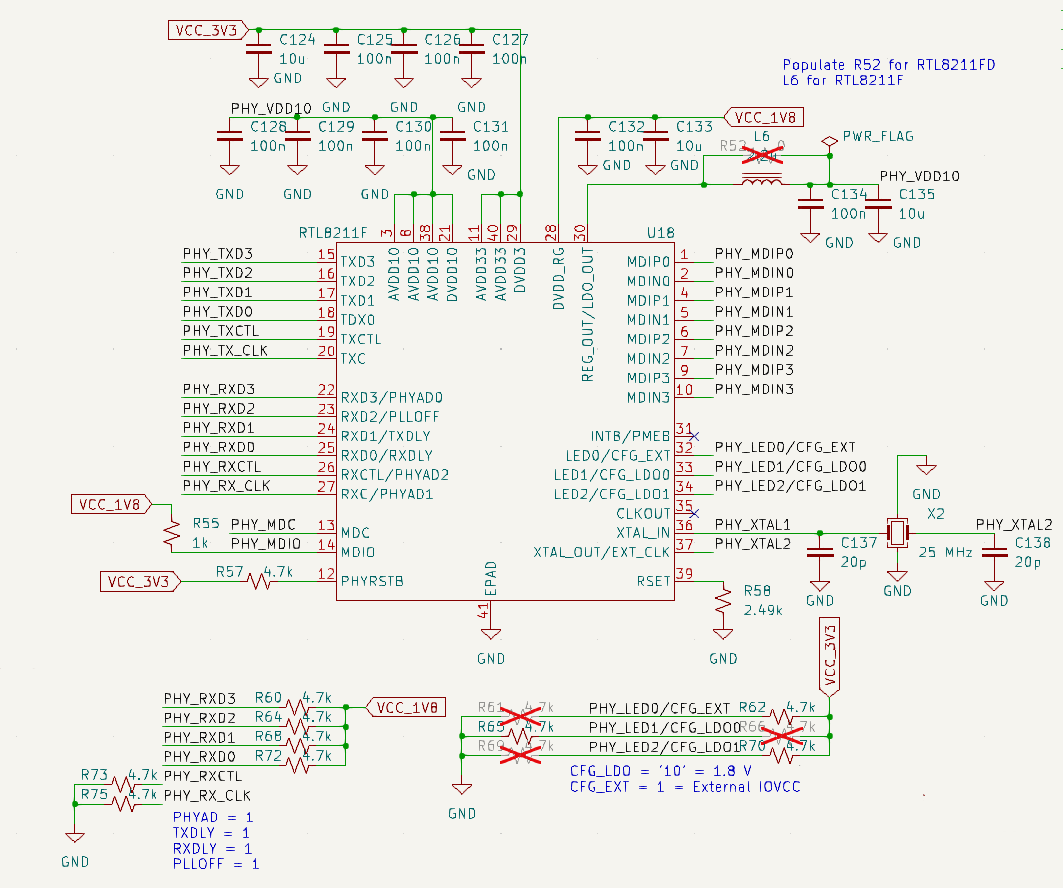
Ethernet chip schematic connections. The chip requires several configuration resistors.
The Ethernet interface needs an external PHY chip that is between the Ethernet connector and the FPGA. The cheapest one I could find was Realtek RTL8211F, which can be found for $1 in single quantities from China. While the RTL8211E version of the chip is found on many FPGA development boards, the F version is much more uncommon. The challenge with this chip is that officially the datasheet is provided only under NDA. However, it is available from the Chinese resellers with big "Confidential" and "Not for public release" labels. However, the datasheet isn't quite clear on how it should be connected, and there aren't any example schematics in it. Searching this chip on Google, I did find few schematics of boards using it, which gave me some confidence that I can wire it correctly. See the above schematic on how it should be wired for FPGA if you are also looking to use it.
Important note about the Zynq FPGA is that the Ethernet interface doesn't meet the RGMII interface (FPGA to Ethernet chip interface) specifications when used with 3.3 V supply voltage. Because of this, I had to set the FPGA PS side supply voltage to 1.8 V, which requires adding level shifters for SD card and UART that are powered from the same voltage.
JTAG and debug UART
FPGA is programmed and debugged with JTAG connection. On development boards there is usually a connector and external JTAG debugger is used to connect to the development board. The official JTAG debugger is quite expensive with $270 list price and I don't want to pay for one.
FTDI makes FT2232H chip that can convert from USB to JTAG and UART. This can be used to implement the JTAG interface cheaper. There used to be a drawback that it wasn't supported by the Xilinx official tools which made debugging the design much harder, but now it's officially supported if the EEPROM memory is programmed with tool provided by Xilinx.
FT2232H also has UART output that is useful for debugging the ARM processor code. Calling printf in the processor code prints characters to the debug UART.
Clock generator

Simplified block diagram of clock signals.
Accurate timing of the whole system is very important. Several clock signals are unavoidable since the ADC runs on 250 MHz, the DAC runs at 500 MHz, and the FPGA requires even lower clock frequency. The FPGA does have several phase-locked loops that can be used to generate clocks, but accuracy of their output isn't good enough. For a 100 MHz clock the tools predict a peak-to-peak jitter of 130 ps, while the clock generator chip has about 4 ps peak-to-peak jitter. ADC and DAC require very clean clocks with minimal jitter, and any timing error on the sampling clock reduces the signal-to-noise ratio.
Everything involved in the radar signal generation or processing should run on synchronized clock signals. For example, if the ADC and DAC would run with completely unrelated clocks, the pulses wouldn't stay synchronized in phase as the clocks would slightly drift. Phase drift would make coherent summing of multiple pulses impossible and seriously harm the performance of the radar.
There are two unrelated clocks on the PCB. PS side of the FPGA has its own 33 MHz crystal and it generates clocks for DDR3, CPU, and peripherals from it. 133 MHz bus clock is also generated from it, which is passed to the programmable logic side of the FPGA. The PL side uses an external clock generator chip CDCM6208 to generate several 250 MHz and 500 MHz clocks from a single 25 MHz crystal. These clocks are all phase synchronized to each other. The PS side's own independent clock is that on power up the clock generator has not been programmed yet. The PS side has its own independent clock, which is needed for programming the clock generator. The independent clock domains of PS and PL don't cause issues with proper clock domain crossings.
The ADC outputs a 250 MHz clock with the data to the FPGA, which is internally divided by two and used to clock the pulse timing logic. This makes the FPGA logic also synchronized to the clock generator. Frequency division is required because 250 MHz clock is too fast for the FPGA logic. The clock division makes that for each 125 MHz clock cycle, two ADC samples are received from both channels for total of 48 bits of data. There is a FIFO for clock domain crossing to the PS side's 133 MHz, and DMA transfers the samples through a 64-bit AXI bus to the DDR3 memory. 133 MHz is used because it needs to be faster than the 125 MHz input clock and this clock needs to be generated by PS so it can't be the PL 125 MHz clock.
The FPGA needs to output a 500 MHz clock with the data to the DAC, and for this purpose, a 500 MHz signal is routed to the FPGA. The FPGA has internal clock generators, but they are not used for this purpose because their jitter is too high. 500 MHz is too high frequency to route on the global clock network of the FPGA, but it's possible to route it on the I/O clock network that is only routed to the I/O buffers. That means no logic can be clocked at 500 MHz, but the chip has serdes that can be clocked from the I/O clock at each pin, which can take four bits at the rising edge of the 250 MHz clock and output them at both rising and falling edges of the 500 MHz I/O clock.
Manufacturing
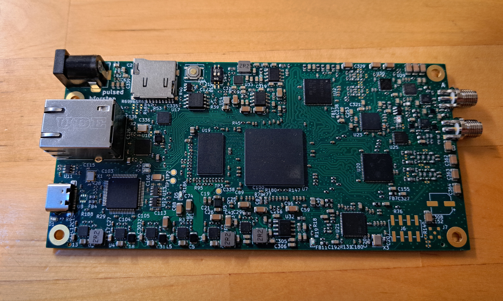
Half populated PCB received from the PCB manufactuer.
I ordered the PCB from a Chinese manufacturer, including assembly. They sent me two assembled pieces and three empty PCBs. Some uncommon components were not available for assembly, and I had to order those separately and solder them myself. These included all the most expensive components such as ADC, DAC and PLL. Luckily, the FPGA was available for assembly, which saved me the trouble of soldering the large 484-pin BGA package myself.
Quality of the PCB looks good, especially considering the price, which is only a fraction of what it would have costed me locally. However, only one of the two assembled PCBs worked out of the box because of soldering issue with one of them.
The suspiciously cheap $15 FPGA had equally suspiciously date and lot codes covered (white rectangles on the FPGA chip in the picture above). I have a development board of the same series chip with markings intact, so it definitely shouldn't look like this. It did end up working, but I wonder what the origin of these chips is.
Fully populated PCB.
I soldered the rest of the components myself using solder paste and hot air tool. It would be difficult to solder the QFN packages without hot air tool on already populated board.
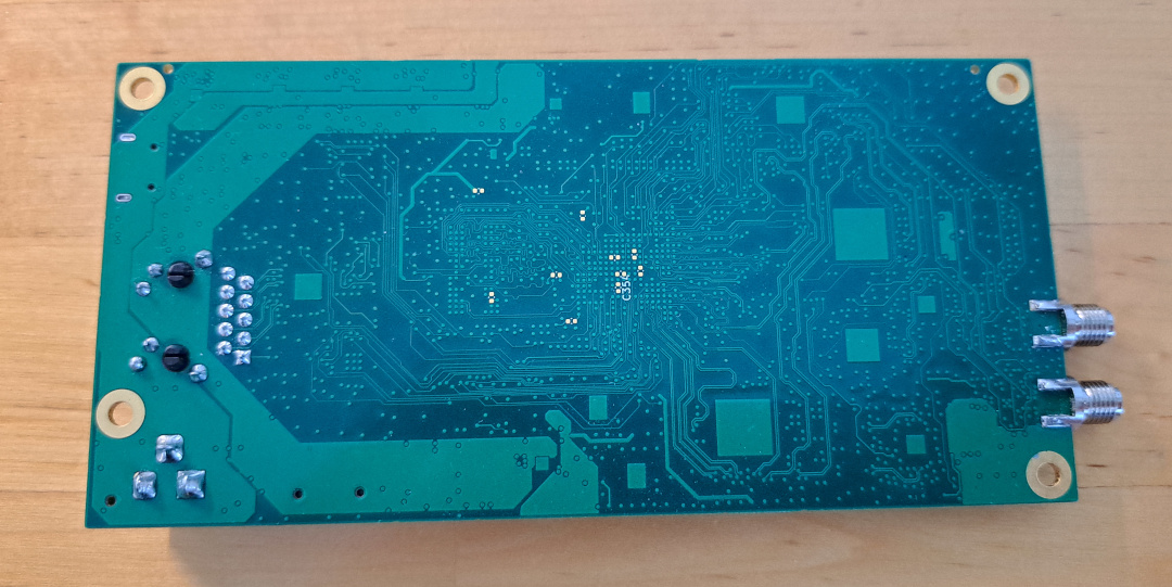
Backside of the PCB.
Two-sided assembly would have costed extra, so all the components are placed only on the top side. There are some places for additional decoupling capacitors on the bottom side just in case, but those were not needed.
JTAG programmer
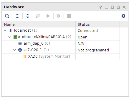
Vivado hardware manager. ARM processor, Zynq 7020 FPGA connected to FTDI chip connected to localhost.
The first step to bring up the board is to program the FT2232H chip, which functions as JTAG programmer and serial port. Xilinx has program_ftdi tool that can program its EEPROM so that Xilinx tools recognize it. I first had problems with the tool not recognizing the device. It failed to find the ftdi device, even though I could see it in the Linux system log. After installing some ftdi libraries and making sure that the official ftdi tools were able to read the EEPROM, I was able to successfully program the EEPROM with the program_ftdi tool.
Checking the Xilinx Vivado hardware manager, it's now able to find the Zynq 7020 FPGA. Programming and debugging the FPGA now works with the Xilinx tools.
FPGA programming

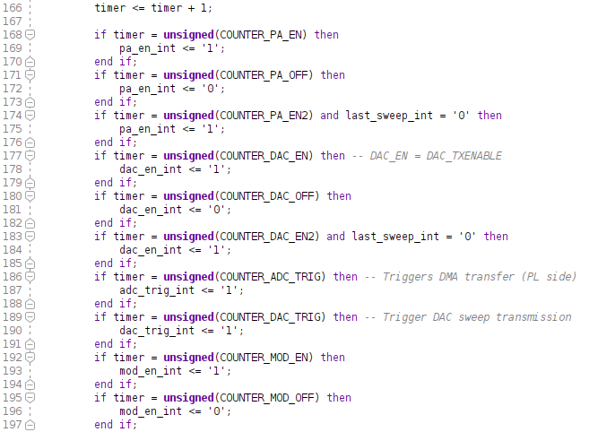
FPGA programmable logic block diagram.
FPGA software consists of ADC and DAC LVDS interfaces, pulse timing that enables and disables switches, PA, LNAs and other components at the right time, AXI registers that enable the PS to configure the programmable logic, two DMA channels for ADC and DAC samples, and SPI interfaces for ADC, DAC, PLL, and clock generator.
Most of the signal processing is done on the PC, and the FPGA mainly passes the data around. However, it would be a good idea to have digital filtering and decimation for the received samples on the FPGA. When the transmitted pulse bandwidth isn't very large, for example when it isn't centered at zero frequency, it's possible to do mixing digitally, filter the samples, and reduce the sample rate. This would enable reducing the amount of data that needs to be sent to PC and increase the frame rate of the radar.
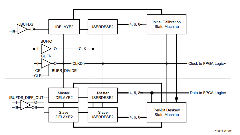
LVDS receiver. Source: xapp1017
LVDS receiver is based on Xilinx appnote xapp1017. It connects two delay lines and flip-flops to each LVDS lane with delay difference set so that they sample the signal with 1/2 bit delay. State machine changes the delays so that the master flip-flop samples at the center of the data eye. The dynamically adjusted delay is able to compensate for PCB routing and FPGA internal delay differences.
Part of the radar pulse timing circuit VHDL code.
The pulse timing circuit is just a counter with equality comparisons for each possible event that can be programmed with AXI registers. The timing circuit is triggered from the PS side of the FPGA, starting the counter that triggers every subsystem on the FPGA and every external chip at the exact correct clock cycle. It also has a loop functionality that can trigger the pulse multiple times with precise repetition interval to support sending a burst of pulses.
Accurate timing of the burst is essential for accurate target velocity measurement. Any timing inaccuracy between ADC and DAC transfers to inaccuracy in the measured distance. A single 125 MHz clock cycle timing error in ADC or DAC triggering translates to a 1.2 m error in the measured distance.
Receiver noise
Testing the radar without antennas.
For bench top testing I put matched loads at the antenna connectors, disabled transmitter and recorded the ADC output. Ideally the recorded signal would be noise and any signals visible are unwanted interference.
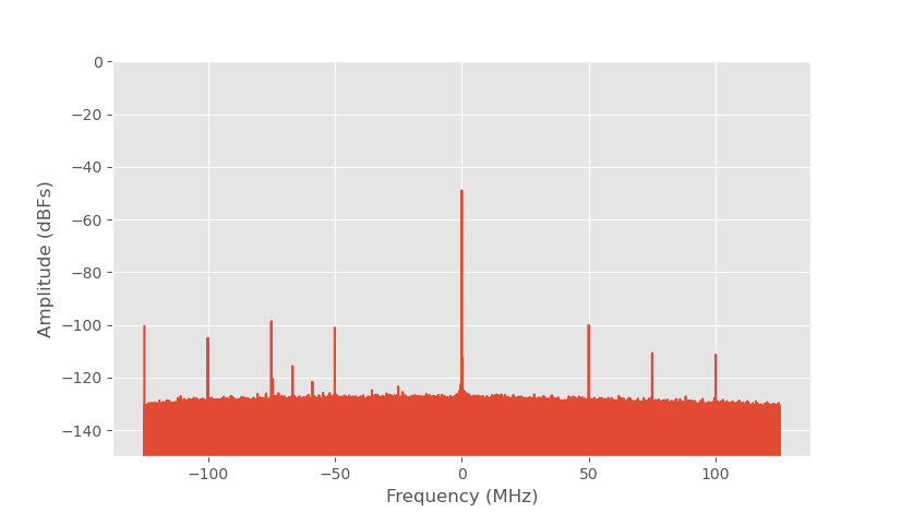
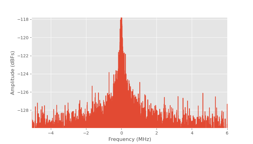
ADC output spectrum without signal, 5.80 GHz LO.
The length of the recording is 33 ms which is 8 million samples. The noise floor average is -139 dBFs which is about what it should be. However, there are several interference signals visible, the biggest are multiples of 25 MHz. Their amplitude is about -100 dBFs which corresponds to about 15 µV RMS at ADC input, so they aren't very large. DC offset of the ADC is also visible as very large peak at zero frequency.
The source of the interferences is fractional spurs caused by the PLL. They can be changed by changing the PLL output frequency, PLL settings and LO input reference frequency.
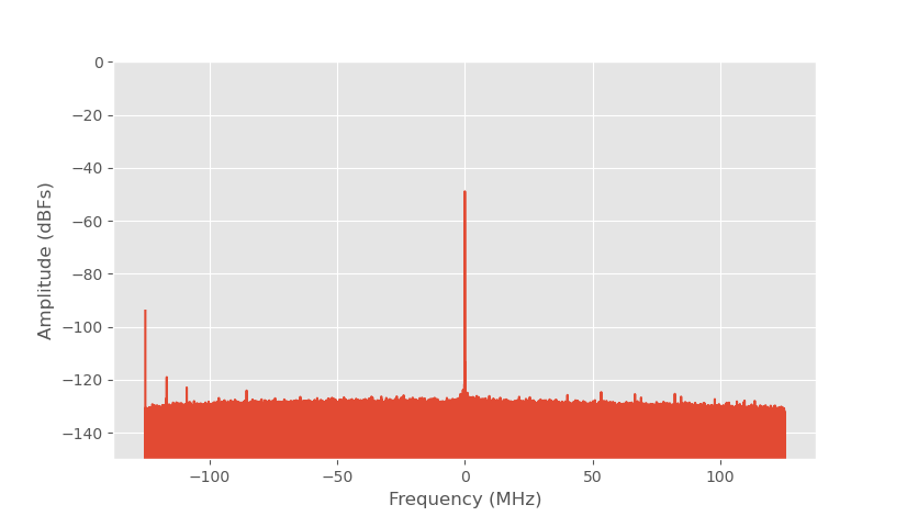
ADC output spectrum without signal, 5.75 GHz LO.
The spurs are minimized when PLL output frequency is integer multiple of the PLL reference clock. PLL reference clock is 250 MHz, but this is too high speed to run the PLL phase detector, and it is divided by two by the PLL reference input divider. With 125 MHz PLL reference clock setting the output frequency to 5.75 GHz makes it integer multiple and almost completely gets rid of the spurs. 5.875 is another close multiple that works well also with RF electronic side. There is still a spur at -125 MHz, but this is expected as it is the phase detector frequency.
ADC output spectrum low frequencies.
Noise floor of the ADC is higher at low frequencies due to 1/f noise of the ADC. Switching frequency of the DC/DC converters is 2.5 MHz and it's not visible at the output spectrum plot, which means that the supply filtering works as designed.
Transmit power
The power amplifier I'm using has an integrated power detector. I set the DAC output voltage to 85% of maximum amplitude, which is about the maximum amplitude it can go while leaving some room for DC offset for LO leakage cancellation digital predistortion. This should result in around +3 dBm output power from the IQ modulator, and with 32 dB power amplifier gain it should be enough to drive the PA into compression.
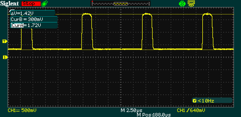
PA power detector voltage measured on oscilloscope.
The power detector pin waveform looks correct when measured on oscilloscope. It has a series of 2 µs long pulses, which was the pulse width. Peak voltage is 1.72 V and about 0.32 V when not transmitting.
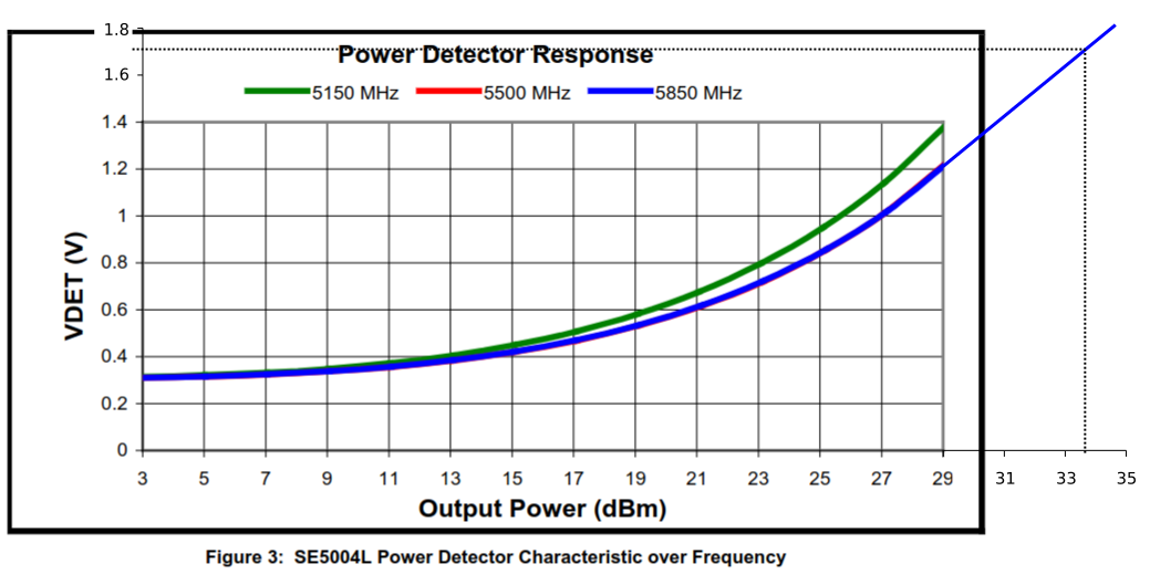
Power detector pin voltage vs output power from the datasheet.
Datasheet has a plot of expected power detector pin voltage vs output power at different frequencies, but the plot doesn't go as high as I measured. Questionable linear extrapolation gives around 33 dBm output power which is two Watts. -1 dB compression point of the PA is specified to be 34 dBm typical, and it looks like it's in compression as expected.
Calibration

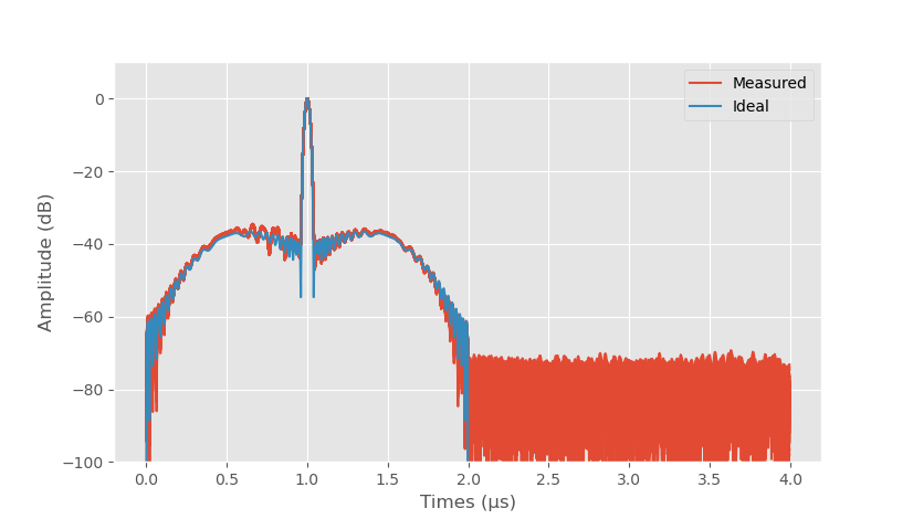
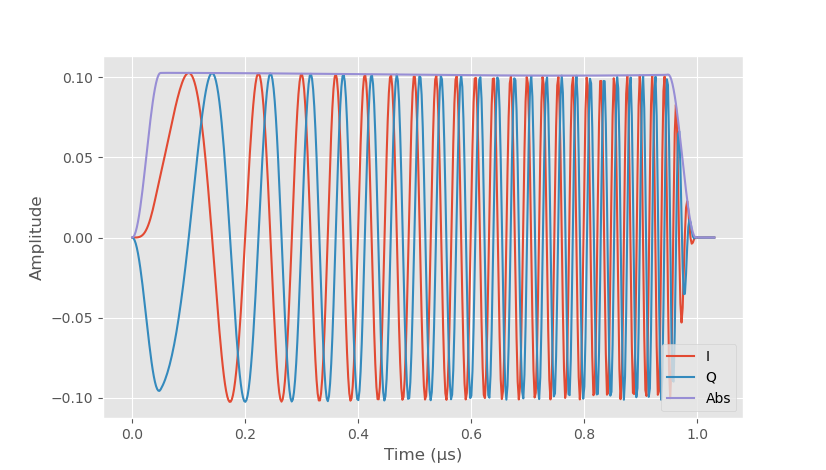
Transmitted waveform.
With matched loads at the antenna connectors I recorded the leakage transmitter signal through the T/R switch. The transmitted waveform is a 100 MHz bandwidth 1 µs long linear frequency sweep with 0.1 of the maximum DAC amplitude.
The baseband frequency sweep signal can be written:
,where \(B\) is bandwidth, \(t_s\) is the sweep length, \(t\) is time, and \(j = \sqrt{-1}\).
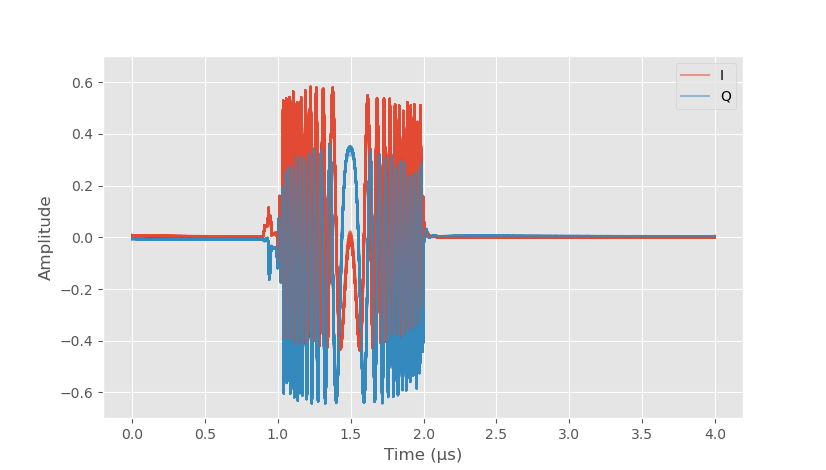
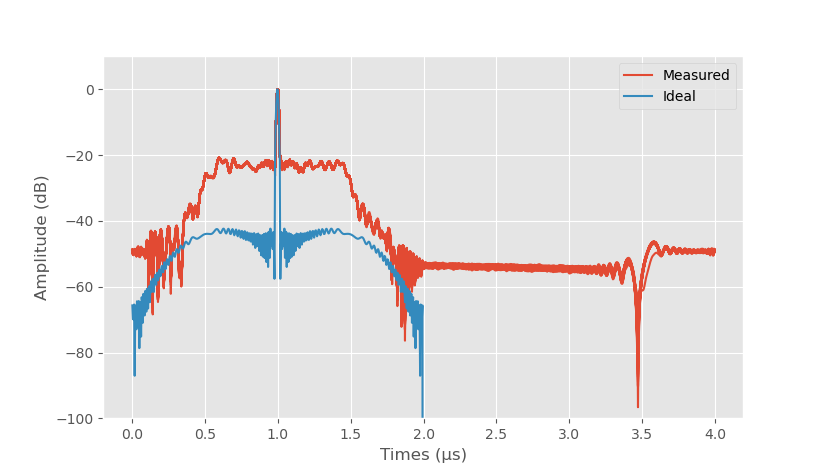
Received frequency sweep without any correction. 128 overlapping waveforms.
The receiver was set to record 1 µs before and 2 µs after the transmitted signal. 128 waveforms were transmitted with very good repeatability with all of them plotted on top of each other on the graph. Ideally the received signal would be attenuated, delayed and phase shifted copy of the transmitted signal, but there is a clear difference between transmitted and received waveforms.
The non-idealities identifiable from the time-domain data are:
- Non-zero DC level before the pulse. This is caused by the DC offset of the ADC.
- Spike before 1 µs caused by the transmitter being switched on.
- Pulse has DC offset caused by the LO leakage from the transmitter, I signal has higher DC level than Q signal.
- Higher baseband frequencies are attenuated more causing a slight drop at the edges of the pulse envelope.
- Non-zero DC level after the pulse. Caused both by the ADC DC offset and ADC filter high-pass behaviour.
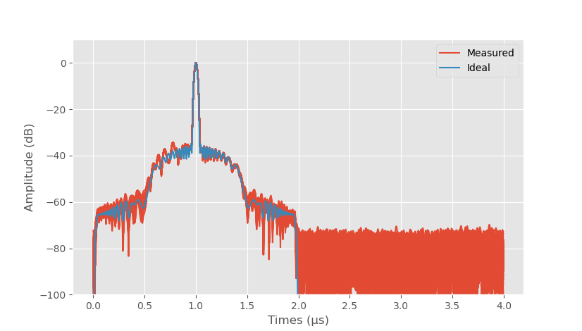
Compressed leakage signal.
Above is the plot of the pulse compression output of the non-calibrated pulse with -50 dB Taylor window applied to the reference pulse normalized to the peak level. The sidelobe level is -21 dBc, which is far above the ideal level.
The biggest error is caused by the LO leakage from the transmitter. LO leakage from the transmitter is mixed down to DC at the receiver because they share the same LO signal. Since DC level of the balanced linear frequency sweep is non-zero, convolution with the reference sweep gives non-zero result wherever there is a non-zero LO leakage that causes the flat correlation output from 0.5 µs to 1.5 µs.
To improve the sidelobe level LO leakage needs to be compensated. It can be done by adjusting the transmitter waveform so that it has LO signal in opposite phase that cancels the leakage signal. However, before LO leakage compensation ADC DC offset should be compensated since received is used to measure the LO leakage and DC offset of the ADC interferes with it.
DC offset of the ADC is compensated by only triggering the receiver with transmitter disabled. The only signal at the ADC is thermal noise and DC offset. DC level can be measured and subtracted from all subsequent measurements.
With ADC DC offset compensated the LO leakage can be measured by triggering the sweep and outputting only zeros from DAC. Ideally there shouldn't be anything transmitted, but due to LO leakage there is signal transmitted at LO frequency which mixes down to DC at the receiver. DC level of the transmitted signal is adjusted such that the ADC input is zero which results in zero LO leakage.
Compressed leakage signal after LO leakage compensation.
With LO leakage compensation the impulse response looks much nicer. Sidelobe level is -36 dB which is few dB above the ideal -42 dB. There is also a very long -60 dB straight line after the sweep that is caused by the high pass behaviour of the AC coupling capacitors between IQ demodulator and ADC.
Time domain leakage signal with LO compensations. DC level after the pulse is very slightly above zero on I channel.
The reason for the long flat part is that there is a non-zero DC level after the sweep. Baseband frequency sweep has non-zero DC component and when it passes through the high-pass filter it changes the output DC level. Convolution result of frequency sweep with a constant results in non-zero output.
The issue could be reduced by decreasing the high-pass filter cutoff frequency. The AC coupling capacitor is only 100 nF which puts the high-pass cutoff frequency at about 10 kHz. DC offset caused by the high-pass could be also compensated digitally.
The decrease in amplitude as frequency increases is quite clear here. DAC sinc response is compensated digitally, so that isn't the cause for the amplitude drop. The ADC filter was supposed to be quite flat in amplitude, but during manufacturing I had to substitute a different inductor than what I initially chose to use. The substitute inductor has higher series resistance and amplitude isn't as flat. I do have the correct inductors, but I haven't replaced them yet.
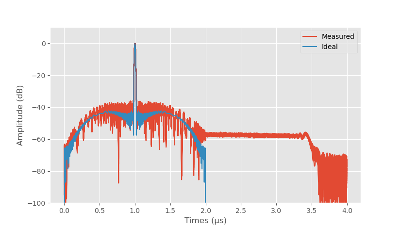
50 MHz frequency sweep with 25 MHz offset.
Other solution for the DC offset issue is modulating the frequency sweep so that sweep doesn't include zero frequency, essentially using non-zero IF. Above is time domain plot of received 50 MHz sweep with 25 MHz offset. Frequency sweeps from 0 Hz to 50 MHz compared to -50 MHz to +50 MHz before.
Compressed sweep with offset.
Calculating the pulse compression of the offset sweep gives much cleaner result. The DC offset issue caused by the high-pass filter is completely removed. Sidelobe level is still 2 dB higher than ideal but this is already quite nice looking impulse response. Ideal sidelobes are higher than with 100 MHz sweep because time-bandwidth product is lower and mainlobe is also widened because of the lower bandwidth. The disadvantage of the modulated sweep is that maximum usable bandwidth of the sweep is half of what can be used with a zero centered sweep.
Transmitted signal with Tukey window with α=0.1.
Sidelobes caused by low time-bandwidth product of the pulse can be reduced with transmitted pulse windowing. Window function reduces the effective bandwidth of the transmitted waveform, so it increases the mainlobe width and reduces the range resolution. Transmitter side windowing also decreases the average energy per pulse as the waveform is tapered off at the start and end of the pulse which decreases signal-to-noise ratio. One good windowing function for transmitter side is Tukey window. It just slightly tapers beginning and end of the waveform with middle being at the maximum amplitude. Tukey window has a parameter α that can be used to control how much it windows, with α=0 being equal to no windowing. With α=0.1 the pulse energy, and the receiver SNR, is decreased by 0.8 dB.
Pulse compressed 50 MHz bandwidth pulse with 25 MHz offset frequency, α=0.1 TX Tukey window, and -50 dB RX Taylor window.
Compared to the same pulse without TX window adding Tukey window to the transmitter greatly decreases the far-away sidelobes. At 500 ns offset the sidelobe level has decreased by about 20 dB. The measured sidelobe level is slightly higher than what it should be ideally.
Receiver and transmitter IQ imbalance isn't yet calibrated and there is some frequency dependent distortion from the ADC and DAC filters. However, the current level is good enough for now.
TX noise leakage

If PA is not disabled during the reception noise from PA output leaks into receiver increasing the receiver noise floor.
When switching to reception T/R switch is switched from transmitter to receiver. If PA is kept enabled due to its high gain it has high enough output noise that even when with attenuation from the switch isolation it's still larger than the thermal noise floor of the LNA.
T/R switch can be switched in about 50 nanoseconds but enabling and disabling PA is much slower, it takes about 10 µs. Unfortunately this long PA switching time means that when using a single antenna the receiver noise is higher due to leaked PA noise.
If the input to PA is thermal noise of 50 ohm resistor (-174 dBm/Hz) it's amplified by PAs gain of 32 dB and it adds its own noise to it too. Usually amplifiers noise figure would be reported in the datasheet but this PA doesn't have it listed. PA noise figure can be rather high, 5 - 10 dB wouldn't be too unusual, as they usually aren't optimized to be particularly low noise. With these figures the noise floor at the PA output is about -135 dBm/Hz. T/R switch has limited isolation, exact value for leakage between these ports isn't reported in the datasheet, but 26 dB is the reported typical isolation to the antenna port and isolation between the input ports is usually little better. This means that PA noise at the LNA input is about -165 dBm/Hz which is larger than the thermal noise floor of -174 dBm/Hz and the PA noise limits the receiver performance if it's not switched off.
Noise figure of the receiver is about 5 dB, so the measured noise floor with receiver connected to T/R switch should be about 5 dB higher, instead of calculated 10 dB with noiseless receiver. Actually measuring the ADC noise floor with PA on, when the receiver is connected to T/R switch the noise floor is 2.1 dB higher than when it's connected to the other port. It matches well with the theory considering the big uncertainties in all of the values.
When using two antennas the second receiver switch can be switched to RX2 and the LNA on the RX1 can be switched off which improves the isolation sufficiently that PA leakage doesn't affect the receiver noise.
Target detection
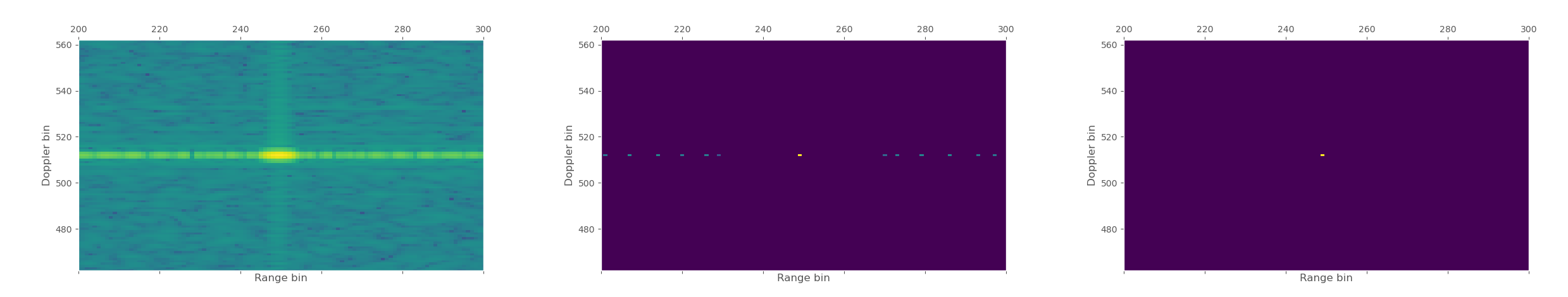
Detecting target from range-Doppler map with CFAR. Range-Doppler map (left), CFAR output (middle), sidelobes filtered out (right). Range on x-axis and Doppler velocity on y-axis.
To get from ADC samples to target detections some more software is required. In general the transmitted signal is a burst of pulses and the first step is to pulse compress each received pulse. After pulse compression the next step is to take FFT over the number of pulses dimension. This sums the power from the different pulses according to velocity of the target. This is called range-Doppler processing and its output is a 2D image with range on one axis and Doppler velocity on the other. Amplitude of each pixel corresponds to the amount of power received at that distance and velocity.
After range-Doppler processing the output is a 2D array of the received power for each range-Doppler bin. To get to target detections we need to identify the bins where there is a target. We also want to separate interesting targets such as moving vehicles from non-interesting targets (clutter) such as sidelobes, trees, ground, and other stationary targets.
The targets in the range-Doppler map could be identified by the amplitude. If a bin's amplitude is high enough above the noise floor then it likely corresponds to a real target and is not just noise. The detection threshold, how much a target needs to be above the noise floor, needs to be chosen to balance false alarm rate and missed detections. In general the noise floor power isn't constant in the range-Doppler map. It can vary as function of time, there can be sidelobes from other nearby targets and clutter, for example ground reflections, can also be considered noise since we don't want to detect each patch of ground as a target. Instead of setting a fixed noise floor it's estimated by averaging nearby bins. For each pixel in the radar map, noise floor is calculated by averaging nearby bins and if amplitude of the bin being tested is larger than threshold times the calculated noise floor then we mark detected target at that location. This is called CFAR (Constant False Alarm Rate) algorithm.
For high amplitude targets there are going to be false detections from sidelobes. After the targets are detected we check if they correspond to a sidelobe of a larger target and unmark it. This is simply done by checking if there is a much larger target in same row or column. Target is also required to have larger amplitude than adjacent bins, this causes only the peak location of each compressed pulse to be detected.
We now have a list of ranges and velocities for detected targets at the accuracy of the radar resolution. Range and velocity measurement accuracy can be improved by interpolating the peak location.
Target tracking

Kalman filter for radar target tracking. Kalman filter predicts the next position of the target from the previous measurements including the uncertainty.
After the detection pipeline we have a list of detections, some of which can be false detections. To be able to track objects in time, detections need to be associated with targets. Kalman filter is used to track each target's position and velocity including uncertainty, and it provides a way to assign each detection to specific target by considering probabilities that detection is from that target.
Tracking uses Stonesoup Python library, which is a library for general object tracking. Specifically radar tracking is heavily based on the StoneSoup tutorial. StoneSoup tutorial explains the tracking well, so I won't repeat it too much here.
The biggest change from the example is that example is for tracking object in 2D with measurement providing it's 2D position but not velocity. Radar measures distance and velocity of each target, but there is no angle information so only 1D tracking is possible.
Transition model for the target is set as constant acceleration. Kalman filter estimates acceleration from the measurements and the next prediction for the target position is made assuming that acceleration is constant.
Radar measurements
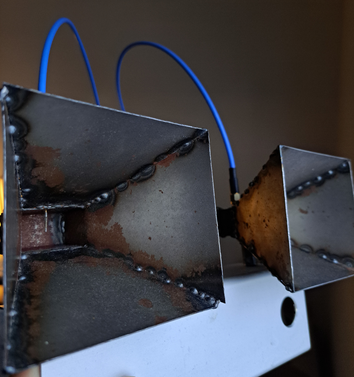
Horn antennas. The rust can't be good for efficiency.
I tested the radar by setting the radar on a side of a road and measuring traffic passing by. Pulse length is 2 µs, the bandwidth is 150 MHz, the number of pulses is 1024, RX length is 5 µs with 7 µs delay before the next pulse. I used two antennas with separate TX and RX antenna. Antennas are horn antennas that I made myself.
150 MHz bandwidth corresponds to 1 meter distance resolution. It's important to note that resolution is not the same as accuracy. Resolution is how close two point targets can be to be separated in the measurement. One target can be measured with better accuracy than resolution with accuracy depending on signal-to-noise ratio.
12 µs time between pulses equals 83 kHz pulse repetition frequency. The pulse interval determines the maximum unambiguous target velocity. Velocity measurement is based on measuring phase change between pulses, and if target moves at high enough speed that it moves several wavelengths between pulses, there is no way for radar to know what that multiple is, causing the measured velocity to be ambiguous.
If the target moves half a wavelength between pulses, it causes a full wavelength distance change since the radar pulse goes from the radar to the target and back. At this speed, the phase increases by a full wavelength at each measurement, which looks identical to if the target was stationary. If we don't have information on which direction the target is moving, we also need to consider that a signal increasing 90 degrees in phase every measurement looks identical to a signal that decreases by 270 degrees every measurement. The unambiguous velocity measurement range must be divided by two for negative and positive velocities, resulting in velocity measurement range:
,where \(\lambda\) is RF wavelength and \(t_d\) is pulse repetition interval.
With 5.8 GHz RF frequency and 12 µs pulse repetition interval, the unambiguous velocity measurement range is from -1077 m/s to +1077 m/s. This is over three times the speed of sound, and there won't be any issues with velocity ambiguities when measuring cars.
The Doppler velocity resolution is the unambiguous velocity measurement range divided by the number of pulses, which is 2155 m/s / 1024 = 2.1 m/s in this case. This is the minimum velocity difference that two targets at the same range need to have to be detected as two separate targets. As with the distance accuracy, the velocity measurement accuracy for a single target is better than velocity resolution and improves with signal-to-noise ratio.
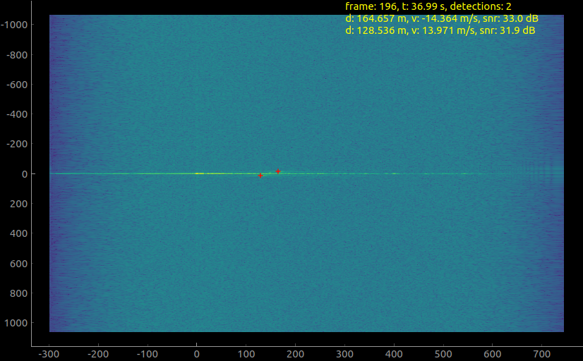
Above is cellphone video synced with a radar range-Doppler map. CFAR detections are plotted as red plus symbols on the range-Doppler map and listed in the order of decreasing SNR on the top right. On the radar image, Y-axis is the Doppler velocity in m/s with negative values towards the radar, X-axis is the distance in meters. The large line at the zero Doppler velocity is reflections from stationary targets.
On the list in the upper right, "frame" is the number of the sweep burst in the radar measurement file, "t" is the time from the first frame, and "detections" is the number of CFAR detections. Detections with a velocity less than 0.1 m/s are filtered out to avoid marking every stationary object as a detection.
Comparing the camera footage to the radar measurements it's easy to correlate the radar detections to cars in the camera footage for close targets. There is some shadowing as cars on the foreground block the view of farther away objects, but the radar is able to detect objects not well visible in the camera footage quite well. The radar can detect cars up to about 400 m, limited by the line of sight. Beyond that the road turns and the view is blocked.
The effect of the DC offset is also visible as very large sidelobes in the range direction. These sidelobes decrease the ability to detect smaller objects near larger ones. Especially towards the end the farthest away car is not always detected by the CFAR as its amplitude isn't sufficiently larger than the sidelobes overlapping it.
Above is the same measurement, but now with Kalman tracker. The tracker assigns CFAR detections to targets with unique IDs. It's able to track multiple targets, but shadowing and sidelobes cause it to not get enough detections from further away blocked targets, and it loses track of them. The uncertainty in their position increases so much that the track deletion threshold is reached. When they become visible again, a new ID is assigned for them. The tracking software could be improved to reduce this problem, but this is just a testing of the radar and I don't want to spend too much time tuning it for this application.
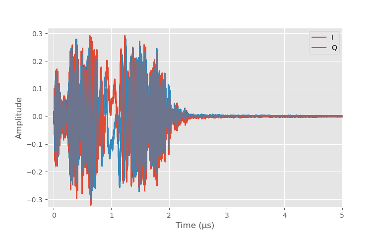
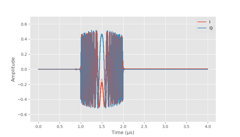
Received signal. 1024 overlapping pulses. Amplitude is normalized to full-scale.
Above is the received signal of all 1024 pulses from one measurement plotted on the same graph. They overlap very well. There is a small change in the phase during the measurement for moving objects, which is enough to separate the moving objects from stationary ones. There is a large return from leakage and nearby objects at the start, and the received signal from longer time delays that correspond to farther away targets are much weaker.
Low-IF pulse
While using a large bandwidth sweep centered at DC works, sidelobes caused by the high-pass filter are visible in the results. For second test, I set the RF bandwidth to 75 MHz with 38 MHz modulation frequency so that the frequency sweeps from 0.5 MHz to 75.5 MHz. Other parameters were kept the same.
This time, as expected, the very wide sidelobes caused by the DC offset aren't visible. Range resolution is only half of what is was previously, but it doesn't really cause any issues with tracking of the cars. They are large enough that even with a 2 meter range resolution, there isn't any issues with separating them.
The frame rate is about only half of what is was before. The amount of data should be the same, and I'm not really sure why it's so much slower this time?
At the beginning, a second reflection of the passing car is visible at double the distance and velocity. The radar signal reflects from car, to a sign that is right next to me, back to car, and then is received by the radar. It's much weaker in amplitude and its spread out which causes it to not be detected as a target by CFAR.
In this measurement, there's a cyclist coming towards the radar which is not detected as a target. The reason for it is that the cyclist's speed isn't large enough to separate it well enough from the stationary targets. When CFAR target detection is calculated, all of the nearby stationary targets are included in the noise floor calculation for low-speed targets. The large noise floor causes that the small radar cross section of the cyclist isn't sufficiently above the noise floor to be detected.
For this application, a higher RF frequency would be beneficial. Doubling the RF frequency would double the Doppler velocity bin separation and decrease the maximum unambiguous Doppler velocity by two. Common police radar speed guns operate at around 10 to 35 GHz, although nowadays lidar, which operates near visible light, is starting to be more common for traffic monitoring.
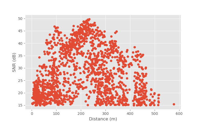
SNR of detected objects as calculated by CFAR vs distance.
SNR of the radar detections is quite good at this range. The maximum SNR at 450 m distance is around 35 dB, while just farther away at 550 m there are no detections. This is because of line of sight, there is no clear path beyond 450 m. Radar SNR should decrease as fourth power of distance, which corresponds to 12 dB drop when the distance is doubled. The radar should be able to detect traffic at even longer distances if there is a clear line of sight.
From this measurement, it isn't clear if the radar link budget is as good as designed, since the radar cross-section of the targets isn't known. Even a typical car cross section can vary a lot depending on the model and the look angle. The radar link budget could be verified by measuring a target with a known radar cross section, typically a corner reflector. However, I don't have a corner reflector. It wouldn't be too difficult to make one with few triangular pieces of PCB, and it just would require some effort.
Full range-doppler map.
The unzoomed range-Doppler map shows how small the view on the videos is on the Doppler axis. The maximum unambiguous velocity is over 1000 m/s. On the range direction, negative distances correspond to pulses that arrive before the start of the transmitted pulse. There shouldn't be any signal there except for sidelobes from targets at positive distances. The noise floor drops at the edges of the range direction because of zero padding in pulse compression.
Single antenna
The previous measurements were made with two antennas, one transmitting and the other receiving. In the next measurement, I have only one antenna that is switched between transmit and receive modes. The pulse was set to the same parameters as the low-IF measurement, except for pulse length, which was decreased from 2 µs to 1 µs to improve detection of close objects.
With one antenna, receiver can only be switched on at the earliest just after the end of the transmission. 1 µs at the speed of light is equal to 300 meters, but radar signal needs to travel to the target and back, so minimum distance to receive the full pulse is 150 meters. However, while it isn't possible to receive the full pulse from shorter distances, it's possible to receive a partial pulse. Pulse compression with only a partial pulse reduces distance resolution and SNR, but it should allow detecting targets at much lower distances.
Targets below 150 m distance can be detected but the range resolution worsen quickly to unusable levels. Minimum range that radar can detect targets with these settings is about 40 m. In this plot marker is drawn on the tracker predicted location instead of CFAR detections as before.
The tracker parameters were tuned a little bit for this measurement and the tracking performance is better than in the earlier measurements.
Conclusion
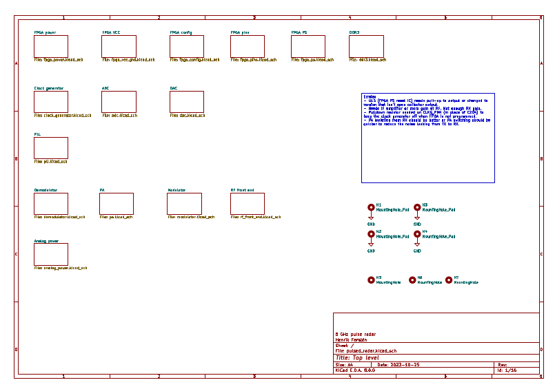
Schematic of the radar.
Schematic of the radar is available. It should be useful for also as a software-defined radio with some modifications or reference for other applications that require FPGA. Firmware and software isn't available at the moment, since I'm not sure if I should make those public.
Cost was 330 USD for PCB manufacturing and assembly of two PCBs and additional 225 EUR (240 USD) for components from Digikey that I soldered myself. This is including 24% VAT and shipping costs. There aren't any similar commercial pulse compression radars in the same price range and even software defined radios with similar RF bandwidth are much more expensive.
The designed radar is fundamentally similar to modern large radars. It utilizes digital signal processing, supports arbitrary waveforms and has very large maximum unambiguous target Doppler velocity due to high pulse repetition frequency. Only the maximum range is shorter than large radars due to low output power and small antenna.